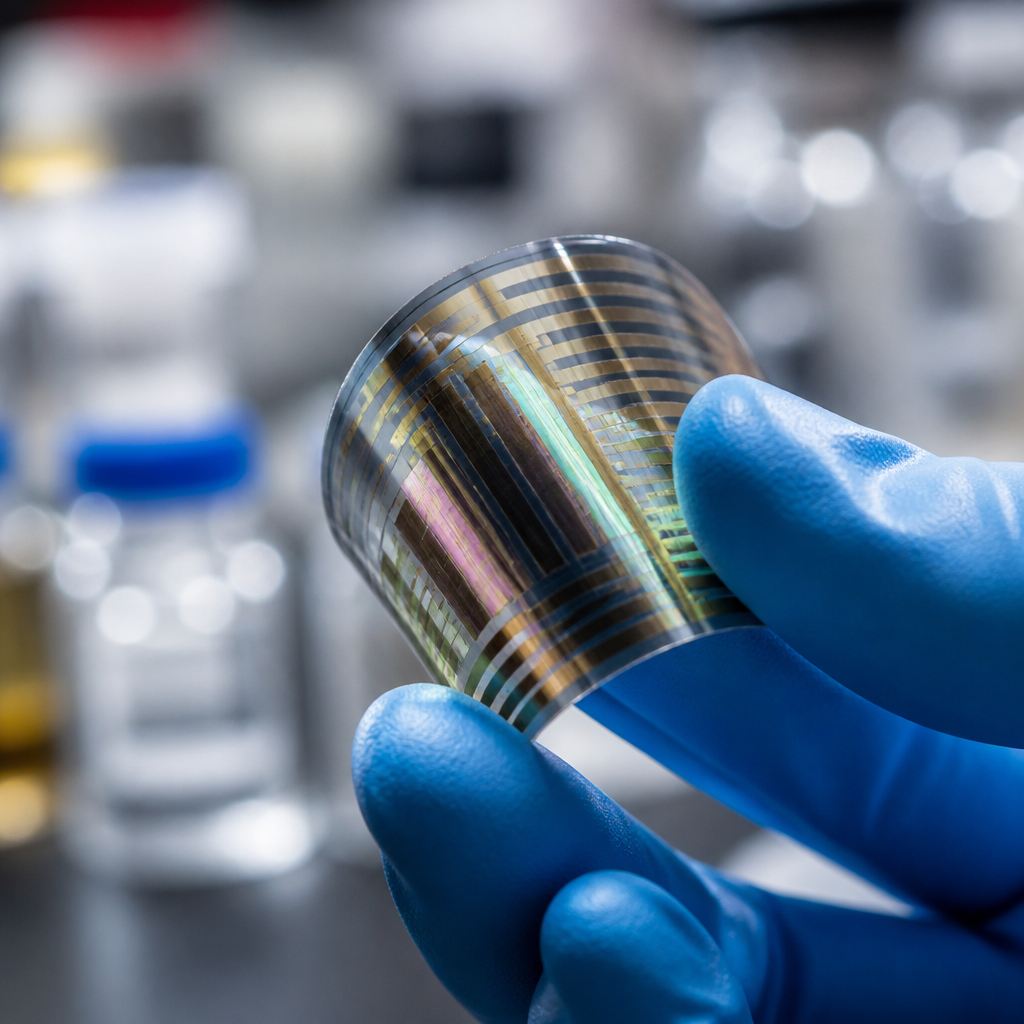
Polymers are moving from passive packaging materials to active optical media, and that shift is redefining optoelectronics. In this field, optoelectronics means devices that convert electrical energy to light or light to electrical signals, including displays, solar cells, photodetectors, waveguides, sensors, and optical communications components. Optical properties describe how a material interacts with light through absorption, transmission, reflection, refraction, scattering, emission, birefringence, and nonlinear response. When engineers discuss the future of polymers in optoelectronics, they are really asking how tunable organic materials can deliver precise optical performance at lower weight, lower processing temperature, larger area, and often lower cost than glass, ceramics, or crystalline semiconductors.
I have worked with polymer films in display stacks and sensor housings, and the practical appeal is obvious the first time a brittle glass concept is replaced by a roll-process film that survives bending, coating, and lamination. Yet performance cannot rest on flexibility alone. For polymers to lead in advanced optoelectronics, their optical properties must be engineered with the same rigor applied to silicon photonics or compound semiconductors. Refractive index control, photoluminescence efficiency, haze suppression, exciton management, and environmental stability are now design variables, not side issues.
This matters because modern products increasingly demand optical function in places where traditional materials struggle. Foldable displays need transparent, low-birefringence barrier layers. Wearable sensors need lightweight substrates that still guide or modulate light. Electric vehicles need robust polymer optics for lidar covers, interior lighting, and human-machine interfaces. Data centers need lower-cost optical interconnect materials. Meanwhile, sustainable manufacturing pressures are pushing the industry toward solution processing, reduced energy input, and recyclable material systems. Polymers sit at the center of these demands because their chemistry can be tuned at the molecular level while their processing can scale through coating, printing, molding, and extrusion.
As the hub for optical properties within materials and properties, this article maps the core concepts that determine polymer performance in optoelectronics and connects them to the most important application areas. It explains what optical parameters matter, how polymer structure affects them, where leading polymer classes excel, and which tradeoffs still limit adoption. Understanding these fundamentals makes it easier to evaluate deeper topics such as refractive index engineering, light extraction, emissive polymers, transparent electrodes, barrier layers, nonlinear optics, and photostability.
How Polymer Structure Controls Optical Properties
The optical behavior of a polymer begins with its molecular architecture. Backbone conjugation determines whether electrons can delocalize and interact strongly with visible or near-infrared light. In conjugated polymers such as polyfluorenes, polythiophenes, and PPV derivatives, alternating single and double bonds create electronic states that support absorption and emission. In nonconjugated optical plastics such as PMMA, polycarbonate, COP, and COC, the main value comes from high transparency, controlled refractive index, low birefringence, and low water uptake rather than active emission.
Crystallinity, chain orientation, and free volume also matter. A highly oriented film may show birefringence, which can distort polarization-sensitive display performance. Excess crystallinity can increase haze through scattering at phase boundaries, while amorphous structures often support better optical clarity. Additives, fillers, and residual solvent can either enhance or damage performance depending on dispersion quality and interfacial compatibility. Even a strong polymer can fail optically if nanoscale phase separation scatters light or if a dopant quenches emission.
Processing history is inseparable from structure. Spin coating, slot-die coating, injection molding, and thermal annealing all influence chain packing and surface roughness. In lab work, I have seen the same polymer formulation shift from clear to visibly hazy simply because drying kinetics changed and trapped microvoids formed. That is why optical properties must be characterized on production-relevant samples, not only ideal films made under slow, controlled conditions.
Key Optical Parameters That Matter in Devices
For transparent polymer components, the first requirement is usually high transmittance across the target wavelength range. Display cover films and encapsulants often need transmittance above 90 percent in the visible spectrum with minimal yellowing. Refractive index is equally important because it determines light confinement, reflection losses, and compatibility with adjacent layers. A mismatch between a polymer substrate and a coating can increase Fresnel reflection and reduce brightness or detector sensitivity.
Absorption coefficient matters in active materials because it controls how effectively a thin film captures photons. In solar cells and photodetectors, strong absorption in the intended band is desirable, but parasitic absorption elsewhere wastes light. Photoluminescence quantum yield is the core metric for emissive polymers used in OLED-related systems, luminescent down-shifting layers, or fluorescent sensors. High quantum yield indicates that absorbed energy is re-emitted efficiently rather than lost as heat through nonradiative decay.
Other critical parameters include haze, birefringence, extinction ratio, optical loss in waveguides, and nonlinear coefficients. A polymer waveguide intended for short-reach data transmission must minimize attenuation from overtone absorption, especially from C-H bonds in the near-infrared. That is why fluorinated polymers have been so important in optical communications research: replacing hydrogen with fluorine reduces absorption losses at telecom wavelengths. For display films, retardation control is central, because even small birefringence errors can shift color and contrast when combined with polarizers.
| Optical property | Why it matters | Representative polymer example | Typical optoelectronic use |
|---|---|---|---|
| Visible transmittance | Controls clarity and brightness | PMMA, COC | Display films, lenses, encapsulation |
| Refractive index | Sets light guiding and reflection behavior | Polycarbonate, sulfur-containing polymers | Waveguides, microlenses, coatings |
| Photoluminescence quantum yield | Measures emission efficiency | Polyfluorenes | Emissive layers, sensing |
| Low birefringence | Preserves polarization performance | COP, COC | LCD optics, AR films |
| Low optical loss at NIR wavelengths | Improves signal transmission | Fluorinated polymers | Optical interconnects, waveguides |
Transparent Polymers for Displays, Lenses, and Light Management
Several polymer families already anchor commercial optical systems. PMMA offers excellent transparency and weatherability, making it common in light guides, automotive lenses, and signage. Polycarbonate provides higher impact resistance and useful refractive index, though it requires careful stabilization against yellowing and scratching. Cyclic olefin polymers and cyclic olefin copolymers stand out for low birefringence, low moisture absorption, and high optical clarity, which is why they appear in advanced display films, diagnostic cartridges, and precision molded optics.
In displays, polymers do more than protect surfaces. They shape light. Diffuser films, prism films, compensation films, optical adhesives, and encapsulants all depend on tightly controlled optical properties. A backlight unit can gain measurable efficiency from polymer microstructures that redirect light toward the viewer. In OLED stacks, optical adhesives must maintain transparency while matching refractive indices and surviving thermal cycling. Flexible displays add another layer of complexity because the polymer must resist crack initiation, maintain low haze under bending, and limit oxygen and moisture permeation that would degrade emissive layers.
Light extraction is a strong example of why optical properties matter at the system level. Many optoelectronic devices trap photons by total internal reflection. Engineers use textured polymer layers, scattering beads, microlens arrays, or graded-index coatings to release more of that trapped light. Gains are often significant because extraction, not generation, is the bottleneck. A well-designed polymer outcoupling film can improve external efficiency without changing the active semiconductor chemistry underneath.
Conjugated and Functional Polymers in Active Optoelectronics
The most transformative future role for polymers lies in active optical function. Conjugated polymers can emit, absorb, transport charge, and respond to external fields. In polymer LEDs, materials such as polyfluorene derivatives and related copolymers have been investigated for color tuning, solution processability, and large-area manufacturing. Although small-molecule OLEDs currently dominate premium displays, polymer emissive systems remain attractive for printed electronics and specialty lighting because they can cover large areas with less complex deposition equipment.
In organic photovoltaics, donor-acceptor polymers have advanced rapidly through bandgap engineering and morphology control. Materials based on benzodithiophene, thiophene, diketopyrrolopyrrole, and related motifs have pushed absorption deeper into the visible and near-infrared while supporting better charge separation. Polymer photodetectors use similar concepts to tune spectral response for imaging, environmental monitoring, and wearable health sensing. The future opportunity is not to replace every inorganic device, but to enable thin, flexible, low-weight platforms where conventional wafers are impractical.
Functional polymers also support electro-optic modulation, nonlinear optics, and responsive sensing. Chromophore-doped polymers can exhibit strong Pockels effect behavior after poling, making them candidates for high-speed modulators. Other systems change fluorescence in response to pH, strain, temperature, or specific analytes, turning optical properties into a direct sensing mechanism. This is especially important in medical patches, food packaging indicators, and structural health monitoring, where conformability and low-cost processing matter as much as sensitivity.
Manufacturing Advantages and Performance Tradeoffs
The strongest argument for polymers is manufacturability. Solution coating, inkjet printing, nanoimprint lithography, injection molding, and roll-to-roll processing allow optical functionality over large areas at comparatively low thermal budgets. That opens doors for flexible solar foils, disposable biosensors, smart labels, and integrated lighting surfaces. Compared with vacuum-heavy fabrication routes, polymer processing can reduce equipment complexity and support rapid iteration of thickness, pattern, and composition.
However, tradeoffs remain unavoidable. Many polymers suffer from lower thermal stability, higher gas permeability, and greater photochemical sensitivity than glass or inorganic semiconductors. UV exposure can break chains or trigger yellowing. Oxygen and water can quench emission and accelerate dark-spot formation in organic devices. Surface hardness is another issue; a beautiful transparent film can still fail commercially if it scratches during assembly or use. These weaknesses do not invalidate polymers, but they require multilayer engineering that combines barrier coatings, stabilizers, crosslinking strategies, and careful interface design.
Standards-based characterization is essential here. Optical transmission is commonly measured with UV-Vis spectroscopy, haze with ASTM D1003 methods, refractive index with ellipsometry or prism coupling, and thermal transitions with DSC or DMA to predict service stability. In development programs, the best decisions come from correlating these measurements with real use conditions such as damp heat, blue-light exposure, and cyclic bending rather than relying on a single headline property.
Where the Future Is Heading
The future of polymers in optoelectronics will be shaped by hybrid design. Instead of asking whether polymers will replace inorganic materials, the better question is where polymers add unique optical value inside mixed material stacks. Expect more polymer interlayers in microLED displays, more printed optical sensors on flexible substrates, more polymer waveguides for board-level interconnects, and more nanocomposite films that combine transparency with tailored index, barrier, or scattering behavior. Researchers are also developing bio-based optical polymers and recyclable thermoplastics to reduce environmental burden without sacrificing clarity.
Artificial intelligence is accelerating materials discovery by screening repeat units, side chains, and processing windows against target optical properties. At the same time, advanced characterization is exposing failure modes earlier, from exciton quenching at interfaces to subtle stress birefringence after lamination. The winners will be materials platforms that pair strong optical performance with durable processing margins. In industry, that usually matters more than chasing a record number on a pristine lab sample.
For anyone evaluating materials and properties in optoelectronics, polymers deserve attention because they combine molecular tunability with manufacturing versatility. Their optical properties can be engineered for transparency, emission, absorption, light guiding, and sensing across applications that demand flexibility and scale. The limits are real, especially in lifetime and environmental stability, but the direction is clear: polymers are becoming core optical materials, not supporting actors. Use this hub as your starting point, then explore deeper topics such as refractive index control, emissive polymer design, waveguide loss, light extraction, and barrier engineering to make better device decisions.
Frequently Asked Questions
1. Why are polymers becoming so important in modern optoelectronics?
Polymers are becoming important in optoelectronics because they are no longer viewed only as protective housings, coatings, or insulating layers. They are increasingly being engineered to function as active optical materials that directly influence how devices generate, guide, detect, and modulate light. That is a major shift for the industry. In optoelectronics, performance depends heavily on how a material absorbs, transmits, reflects, refracts, scatters, or emits light, and advanced polymers can now be tailored at the molecular level to optimize many of those behaviors.
One of the biggest advantages of polymers is design flexibility. Their chemical structure can be modified to tune refractive index, transparency, fluorescence, birefringence, conductivity, and even nonlinear optical response. This makes them attractive for use in displays, organic light-emitting devices, solar cells, photodetectors, waveguides, optical sensors, and communication components. Compared with many traditional inorganic materials, polymers are often lighter, easier to process, and compatible with large-area or flexible manufacturing methods such as printing, coating, lamination, and roll-to-roll fabrication.
That combination of functional tunability and scalable processing is especially valuable as the market moves toward bendable displays, wearable sensors, compact photonic systems, and low-cost optical components. In many cases, polymers enable form factors that would be difficult or expensive to achieve with rigid glass or crystalline semiconductors alone. As a result, the future of optoelectronics is likely to involve hybrid systems in which polymers work alongside inorganic materials, as well as fully polymer-based devices in applications where flexibility, weight, cost, and large-area integration matter most.
2. What optical properties make polymers suitable for devices like displays, solar cells, and waveguides?
The suitability of polymers for optoelectronic applications comes down to a set of optical properties that can be carefully controlled through chemistry, formulation, and processing. Transparency is one of the most important. Many optical devices require materials that transmit light efficiently over specific wavelength ranges, whether visible, ultraviolet, or near-infrared. Polymers can be developed to minimize unwanted absorption and haze, which is essential for display substrates, encapsulation films, lenses, and waveguides.
Refractive index is another key property. In waveguides, optical interconnects, and photonic packaging, precise refractive index control determines how light is confined and directed. Polymers are useful because their index can be adjusted by changing backbone chemistry, side groups, fillers, or copolymer composition. This supports the fabrication of graded-index structures, claddings, and optical layers with customized light-management behavior. Similarly, low scattering is critical in applications where signal loss must be minimized, such as communications components and integrated photonics.
For active optoelectronic devices, light absorption and emission become central. In solar cells and photodetectors, polymers can be designed to absorb selected portions of the spectrum and convert incident photons into electrical signals. In displays and light-emitting devices, emissive polymers can produce light efficiently with tunable color characteristics. Some polymers also exhibit useful birefringence or polarization behavior, which matters in display optics and sensing systems. Others can provide nonlinear optical effects for modulation or switching.
The broader point is that polymers are not defined by a single optical strength. Their real value lies in the ability to engineer multiple properties at once. A polymer can be made transparent, flexible, mechanically robust, and optically functional in a single platform. That kind of property integration is one of the main reasons polymers are gaining ground in next-generation optoelectronic design.
3. How are active optical polymers changing the design of optoelectronic devices?
Active optical polymers are changing device design by allowing the material itself to participate directly in optical conversion, transport, or sensing rather than merely supporting other components. Traditionally, a polymer in an optoelectronic system might have served as an encapsulant, spacer, adhesive, or insulating substrate. Today, polymers can act as light-emitting layers, charge-transport media, photoactive absorbers, optical gain materials, or waveguiding structures. That expands the design space considerably.
In displays, for example, polymer-based emissive materials and transport layers can support thinner, lighter, and more flexible architectures. In solar cells, conjugated polymers can serve as photoactive semiconductors that absorb sunlight and contribute to charge generation. In photodetectors and sensors, functional polymers can be engineered to respond selectively to light intensity, wavelength, polarization, or environmental stimuli, enabling compact and highly tailored sensing platforms. In optical communications, polymer waveguides and modulators can simplify routing and integration while supporting lower-cost fabrication.
Perhaps the most significant impact is on manufacturability and device form factor. Because many active polymers are solution-processable, they can be deposited over large areas and onto flexible substrates. This opens the door to printed electronics, conformal photonic devices, and integrated systems that combine optical and electronic functions in lightweight packages. Designers are no longer limited to rigid, brittle material sets or conventional wafer-based manufacturing approaches.
That said, active optical polymers are not simply replacing all traditional materials. In many high-performance devices, they are being incorporated into hybrid architectures that use the strengths of both polymeric and inorganic components. The future likely belongs to these mixed-material systems, where polymers deliver flexibility, spectral tunability, and process efficiency while other materials contribute exceptional mobility, stability, or high-power operation.
4. What are the biggest challenges limiting wider use of polymers in optoelectronics?
Despite their promise, polymers still face several important challenges before they can achieve broader adoption across the full range of optoelectronic applications. The first is long-term stability. Many polymer systems are sensitive to oxygen, moisture, heat, ultraviolet radiation, or repeated electrical and optical stress. Over time, this can lead to photobleaching, oxidation, loss of transparency, color shifts, efficiency decline, or mechanical degradation. For commercial devices expected to operate reliably for years, stability remains a critical benchmark.
Another challenge is performance consistency. Because polymer properties can be strongly influenced by molecular weight, chain ordering, processing conditions, solvent history, additives, and interfacial structure, maintaining uniform optical and electronic behavior at scale can be difficult. Small variations in fabrication may affect refractive index, absorption spectrum, scattering losses, charge transport, or emission efficiency. This is especially important in applications such as waveguides, displays, and optical communication devices, where tight tolerances are essential.
There are also limitations related to intrinsic material performance. In some cases, polymers may not yet match the thermal endurance, carrier mobility, environmental resistance, or ultra-low optical loss of well-established inorganic materials. For high-power, high-temperature, or extremely low-loss applications, that can restrict where polymers are practical. Encapsulation and barrier technologies help, but they add complexity. In addition, integrating polymers into existing semiconductor and photonics manufacturing flows may require new process windows, compatibility studies, and reliability standards.
Still, these challenges are not signs that polymers are unsuitable for optoelectronics. Rather, they define the current frontier of materials engineering. Researchers are addressing them through improved polymer chemistry, crosslinking strategies, nanocomposites, multilayer barrier systems, better purification, and more controlled processing methods. As those advances continue, the balance between polymer advantages and polymer limitations is shifting steadily in favor of wider adoption.
5. What does the future of polymers in optoelectronics look like over the next decade?
Over the next decade, polymers are likely to play a much larger and more sophisticated role in optoelectronics, especially in applications that benefit from flexibility, lightweight construction, scalable manufacturing, and tunable optical response. We can expect continued growth in flexible and foldable displays, wearable optical sensors, lightweight solar technologies, and integrated photonic components for short-range communications and data handling. In all of these areas, polymers offer a compelling combination of functionality and manufacturability.
A major trend will be the rise of highly engineered polymer systems rather than generic plastics. Future materials will be designed with precise optical targets in mind, such as selective absorption bands, controlled emission color, low-loss light guiding, polarization sensitivity, or switchable refractive behavior. Hybrid materials that combine polymers with nanoparticles, quantum dots, organic semiconductors, or inorganic nanostructures will likely become more common, enabling better efficiency and broader spectral control. This will help push polymers into more demanding roles in sensing, imaging, and photonic integration.
Manufacturing is also expected to evolve. Printable optoelectronics, roll-to-roll production, and low-temperature processing could make it possible to fabricate large-area optical devices more economically than with conventional rigid technologies. That has implications not only for consumer electronics but also for healthcare, automotive systems, smart packaging, building-integrated energy devices, and distributed environmental monitoring. As production methods mature, polymers could help make advanced optoelectronic functionality available in places where cost, weight, or form factor previously created barriers.
In practical terms, the future is not a simple replacement story where polymers displace every legacy material. Instead, polymers are becoming a strategic material class that broadens what optoelectronic devices can do and how they can