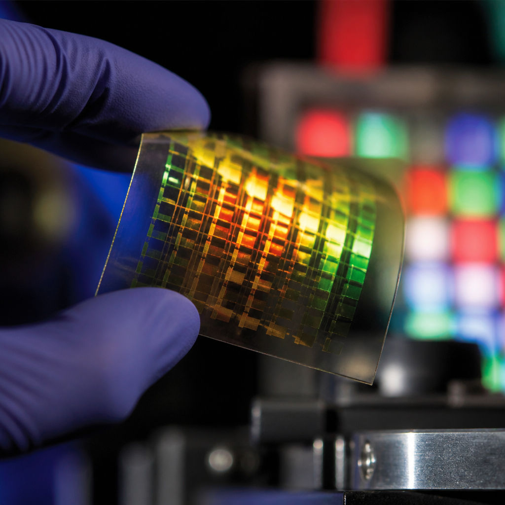
Polymer-based light emitting diodes have moved from laboratory curiosities to strategically important display and lighting technologies because they combine solution-processable materials with tunable optical properties. In practical terms, a polymer LED, often shortened to PLED, is a thin-film device in which a semiconducting polymer emits light when electrical current drives electrons and holes to recombine. The phrase optical properties covers the behaviors that determine how efficiently, accurately, and consistently that emitted light is generated, transported, and perceived, including absorption, photoluminescence, electroluminescence, color purity, refractive index, outcoupling, angular emission, and operational stability. For anyone working within materials and properties, this optical perspective is the hub that connects chemistry, device architecture, processing, testing, and end-use performance.
I have worked with emissive polymer stacks where a small change in solvent choice or annealing temperature shifted peak wavelength by several nanometers and cut brightness uniformity across a panel. That experience makes one point clear: optical performance in polymer LEDs is never just about the emitter itself. It depends on chain packing, energy transfer, interfaces, electrode transparency, and microcavity effects inside the device. These interactions matter because modern applications demand more than visible light. They require high external quantum efficiency, stable chromaticity, low power draw, wide viewing angles, and manufacturability on large or flexible substrates. A display maker cares about saturated red, green, and blue pixels. A sensor designer may care more about narrow spectra or near-infrared response. A lighting engineer may prioritize high luminous efficacy and reduced color shift over lifetime.
Interest in polymer LEDs has also grown because they promise lower-cost fabrication than conventional inorganic LEDs in some formats. Many polymer systems can be deposited by spin coating, slot-die coating, gravure printing, or inkjet printing, which opens paths to lightweight displays, conformable lighting sheets, and integrated photonic surfaces. Yet optical properties remain the main bottleneck between promising materials and commercially robust products. If excitons are quenched by defects, if waveguiding traps most generated photons, or if phase separation broadens the spectrum, the manufacturing advantage does not translate into useful devices. Understanding optical properties therefore means understanding where photons are lost, how spectra evolve, and which innovations are solving those problems. This article maps those innovations comprehensively, so readers can use it as a central reference for deeper work across emissive polymers, transport layers, outcoupling structures, and characterization methods.
How light is generated in polymer LEDs
The basic optical process in a polymer LED begins when an applied voltage injects electrons from the cathode and holes from the anode into an emissive polymer layer. These charges migrate through delocalized molecular orbitals and meet to form bound electron-hole pairs called excitons. When excitons decay radiatively, the device emits photons. The exact emission color depends on the polymer bandgap, conjugation length, local dielectric environment, and the degree of intermolecular interaction. Polyfluorenes, for example, have long been used for blue emission because of their relatively wide bandgaps, while PPV derivatives and donor-acceptor copolymers have been tuned toward green, red, and near-infrared output.
Several optical properties emerge directly from this mechanism. Photoluminescence quantum yield measures how efficiently absorbed light is re-emitted, while electroluminescence efficiency reflects the full electrical-to-optical conversion under device operation. The emission spectrum is described by peak wavelength, full width at half maximum, and Commission Internationale de l’Eclairage coordinates. In a high-performing polymer LED, these values are not accidental. They are engineered by controlling molecular design, film morphology, and optical field distribution. A narrow spectrum supports high color purity for displays. A broader spectrum may suit white lighting when balanced across multiple emitters.
The challenge is that only a fraction of generated excitons become useful external light. Spin statistics in fluorescent systems traditionally limit internal quantum efficiency because many excitons form as triplets that do not radiate efficiently. In addition, generated photons can be reabsorbed by the polymer, trapped in substrate or waveguide modes, or absorbed by electrodes. Innovations in polymer LEDs therefore focus not just on brighter emitters, but on the entire optical path from exciton formation to photon escape. That systems view is essential when evaluating materials and properties.
Material design innovations shaping optical properties
The strongest optical advances in polymer LEDs have come from molecular engineering. Chemists now design conjugated backbones and side chains with a level of precision that directly targets color stability, quantum yield, and solid-state packing. Early polymers often suffered from aggregation-caused quenching, where close chain packing opened non-radiative pathways and red-shifted emission. Newer designs use sterically bulky side groups, twisted backbones, or controlled donor-acceptor sequences to suppress detrimental aggregation while preserving charge transport.
One influential innovation is the development of thermally activated delayed fluorescence concepts in polymer-compatible systems. By minimizing the energy gap between singlet and triplet excited states, these materials allow non-emissive triplets to convert back into emissive singlets through reverse intersystem crossing. In practice, that improves exciton utilization beyond the traditional fluorescent limit. Another important route uses hyperfluorescence-style architectures, where a sensitizing host transfers energy efficiently to a narrowband emitter. Although more established in small-molecule devices, related design logic is increasingly informing polymer systems, especially where spectral purity is critical.
Blue polymer emission remains the hardest target because high-energy excited states accelerate bond scission, oxidation, and spectral instability. Researchers have responded with deeper HOMO levels, more rigid backbones, and reduced keto defect formation in polyfluorene-type systems. For red and near-infrared polymer LEDs, the challenge shifts toward maintaining quantum yield while narrowing the bandgap. Donor-acceptor copolymers can emit at longer wavelengths, but they often experience stronger non-radiative decay because the energy gap law favors vibrational losses. The best recent materials counter this with rigidified structures and reduced conformational disorder.
Crosslinkable polymers are another practical innovation. In multilayer solution processing, one coated layer can dissolve the previous layer unless it is insolubilized. Crosslinking helps preserve interface quality and optical uniformity while enabling more advanced stacks. When the stack is optically cleaner and less intermixed, emission spectra become more reproducible and leakage currents fall. That benefit is especially relevant for printed devices scaled beyond laboratory pixels.
Film morphology, interfaces, and optical loss control
In polymer LEDs, morphology is optical destiny. The same polymer can produce very different spectra and efficiencies depending on chain alignment, phase separation, roughness, and defect density. During process development, I have seen two films made from identical batches show clearly different green shoulders in the spectrum simply because one dried too slowly, allowing domains to aggregate. This is common. Solvent boiling point, drying rate, substrate surface energy, and annealing profile all influence how chains pack in the solid state.
Smooth, pinhole-free films improve charge balance and reduce local quenching. Controlled molecular orientation can also improve outcoupling because horizontally oriented transition dipoles emit more efficiently toward the viewer than vertically oriented ones. While orientation engineering is often discussed with vacuum-deposited emitters, polymer researchers increasingly use side-chain design, alignment layers, and processing additives to steer dipole orientation in solution-cast films. Interfacial layers such as PEDOT:PSS, polyethylenimine derivatives, ZnO nanoparticles, and transition metal oxides further shape optical behavior by affecting recombination zone position and exciton quenching near electrodes.
Optical losses are rarely concentrated in one place. They are distributed across non-radiative recombination, self-absorption, electrode absorption, and waveguiding. Managing them requires coordinated choices across the stack. A highly transparent anode such as indium tin oxide is standard, but its surface roughness and work function must be tuned to protect the emissive layer. Encapsulation also matters optically because oxygen and water ingress create dark spots and oxidized species that absorb or quench light. Barrier films used in flexible devices therefore influence both lifetime and maintained luminance.
| Optical factor | Main cause | Typical effect on device | Common mitigation |
|---|---|---|---|
| Aggregation quenching | Excessive chain packing | Lower quantum yield, red shift | Bulky side chains, host-guest design |
| Waveguide loss | High refractive index contrast | Photons trapped in film or substrate | Microlenses, scattering layers, index matching |
| Electrode absorption | Optical overlap with metal layers | Reduced external efficiency | Transparent electrodes, cavity tuning |
| Self-absorption | Emission overlaps absorption band | Spectrum broadening, lower output | Large Stokes shift materials, thinner films |
| Exciton quenching at interfaces | Recombination too close to electrode or defects | Efficiency loss, faster degradation | Blocking layers, smoother interfaces |
Color purity, white emission, and spectral engineering
Color is where optical properties become visible to end users. For displays, saturated primary colors are essential because wide color gamut standards such as DCI-P3 and Rec. 2020 demand narrow and accurately positioned emission bands. Polymer LEDs historically faced a tradeoff between efficiency and color purity, especially in blue and deep red. Recent spectral engineering strategies address this by reducing conformational disorder, limiting excimer formation, and using energy transfer from a polymer host to a molecular or polymeric dopant with a narrower emission profile. The result is cleaner electroluminescence and lower dependence on operating current.
White polymer LEDs involve a different optimization problem. Instead of narrow single-color emission, they need balanced multicolor output with acceptable color rendering and stable correlated color temperature. Approaches include polymer blends, multilayer emissive regions, and single polymers containing multiple chromophores. Each route brings optical tradeoffs. Blends can separate during aging, shifting the spectrum. Multilayer designs can improve control but complicate solution processing. Single-component white emitters simplify fabrication but often broaden the spectrum in ways that reduce efficacy. In lighting prototypes, the most robust systems usually prioritize stable chromaticity over laboratory peak efficiency because spectral drift is obvious in real rooms.
Microcavity engineering provides another lever for spectral control. By tuning layer thicknesses and reflective interfaces, developers can shape the optical density of states and alter the emitted spectrum and directionality. This can sharpen apparent color or enhance output at targeted wavelengths. The tradeoff is angular dependence. A strongly resonant cavity may produce color shift when viewed off-axis, which is undesirable in large-area displays. The best polymer LED designs therefore use cavity effects carefully, balancing enhancement against viewing-angle uniformity.
Outcoupling, measurement, and the road to practical adoption
Even excellent emissive polymers waste much of their light internally. In a typical planar organic or polymer LED, only about 20 to 30 percent of generated photons escape directly, while the rest are trapped in substrate, waveguide, or surface plasmon modes. Improving light outcoupling is therefore one of the highest-value innovations in polymer LED optics. Practical methods include microlens arrays on the substrate, internal scattering particles, low-index grids, corrugated layers, and refractive-index-matched encapsulants. These structures reduce total internal reflection and redirect trapped modes outward. In pilot lines, outcoupling layers can deliver substantial brightness gains without changing the emissive chemistry, which makes them attractive for scale-up.
Reliable measurement is equally important. Optical properties should be characterized with UV-visible absorption spectroscopy, photoluminescence spectroscopy, integrating-sphere quantum yield measurement, angle-resolved electroluminescence, ellipsometry for refractive index and thickness, atomic force microscopy for morphology correlation, and lifetime tests under controlled current and temperature. External quantum efficiency alone is not enough. A material that starts bright but shifts color or loses half its luminance quickly is not a strong candidate. Industry-relevant testing often follows standards from the CIE and established OLED measurement practice, including reporting luminance, current efficiency, power efficiency, spectral coordinates, and operational lifetime such as LT50.
The commercial path for polymer LEDs is selective rather than universal. They are especially compelling where printing, flexibility, low-temperature processing, or large-area coverage outweigh the absolute peak efficiency of competing technologies. Innovations in optical properties are steadily expanding that window. Better blue emitters, improved triplet harvesting, controlled morphology, and smarter outcoupling are turning polymer LEDs into more predictable engineering platforms. For readers exploring materials and properties, optical behavior is the central thread linking chemistry to performance. Follow that thread into emitter design, interfacial layers, printed manufacturing, and degradation science, and the full logic of polymer LED innovation becomes clearer. Use this hub as your starting point, then dive deeper into each linked subtopic to evaluate which optical strategies best fit your application.
Frequently Asked Questions
1. What are polymer-based light emitting diodes (PLEDs), and how do they work?
Polymer-based light emitting diodes, or PLEDs, are thin-film electronic devices that produce light using semiconducting polymers instead of the small-molecule materials found in many conventional LED and OLED architectures. In a typical PLED, multiple very thin layers are stacked between two electrodes. When voltage is applied, one electrode injects electrons while the other injects holes. These charge carriers move through the polymer layers and eventually meet inside the emissive region. When electrons and holes recombine, they form excited states known as excitons, and as those excitons relax to a lower energy state, light is emitted.
What makes PLEDs especially important is the combination of electronic functionality and material versatility. Because the active materials are polymers, they can often be dissolved in solvents and deposited by solution-based techniques such as spin coating, slot-die coating, inkjet printing, or roll-to-roll processing. That gives manufacturers a potential path to lower-cost, large-area fabrication compared with vacuum-intensive methods. In addition, the optical properties of these polymers can be tuned through molecular design, allowing researchers to influence emission color, brightness, efficiency, and spectral purity. This ability to engineer light output at the chemical level is one of the central reasons PLEDs have evolved from research curiosities into strategically significant technologies for displays, signage, and emerging lighting applications.
2. What recent innovations are improving the performance of polymer-based LEDs?
Recent innovation in PLEDs has focused on solving a set of long-standing challenges: improving charge balance, increasing quantum efficiency, enhancing color purity, extending operational lifetime, and making manufacturing more reliable at scale. One major area of progress is polymer chemistry itself. Researchers are designing new conjugated polymer backbones and side-chain structures that improve charge transport while preserving strong light emission. By controlling molecular packing, energy levels, and film morphology, they can reduce non-radiative losses and increase the likelihood that injected carriers recombine efficiently to emit photons rather than waste energy as heat.
Another important advance involves device architecture. Modern PLEDs increasingly use optimized hole injection layers, electron transport layers, and interlayers that better match the energy levels of the electrodes and the emissive polymer. This helps lower operating voltage and improves charge injection symmetry, which is critical for efficiency and device stability. Innovations in host-guest systems, cross-linkable polymers, and multilayer solution processing have also made it easier to create more sophisticated device stacks without damaging underlying layers during fabrication. On top of that, encapsulation technology has improved significantly, helping protect moisture- and oxygen-sensitive polymers from degradation. Taken together, these innovations are moving PLEDs closer to commercially robust performance, especially in flexible displays, printed electronics, and specialized lighting formats where their processability offers a distinct advantage.
3. Why are tunable optical properties so important in polymer LED technology?
Tunable optical properties are fundamental to the appeal of PLEDs because they allow engineers to tailor how the device emits light for different end uses. In this context, optical properties include emission wavelength, color saturation, luminous efficiency, absorption behavior, refractive characteristics, and how effectively internally generated light escapes the device. By modifying the polymer’s molecular structure, adjusting conjugation length, selecting substituent groups, or blending materials strategically, researchers can control these behaviors with impressive precision. That means a polymer can be designed to emit deep blue for high-resolution displays, warm white for lighting, or highly saturated red and green for color-critical applications.
This tunability also matters for efficiency and visual quality. A material that emits at the right wavelength but suffers from self-absorption, broad spectral output, or poor photoluminescence efficiency may not perform well in a commercial device. As a result, innovation is not just about making a polymer glow; it is about making it emit the right light, in the right amount, with the right stability, and under practical electrical conditions. Researchers are also paying close attention to optical outcoupling, because a substantial portion of generated light can be trapped inside the device due to waveguiding and refractive index mismatches. Improvements in film design, microstructures, and optical layer engineering can help extract more usable light. In short, tunable optical properties are what enable PLEDs to be adapted across a wide range of display and lighting technologies while supporting better performance and more precise product design.
4. What are the biggest challenges still facing polymer-based LEDs?
Despite major progress, PLEDs still face several technical and commercial hurdles. One of the most persistent challenges is operational stability, particularly for blue-emitting materials. Blue PLEDs require wider bandgap polymers, and these materials often degrade faster under electrical stress than red or green emitters. Since full-color displays rely heavily on stable blue performance, this remains a critical issue. Material degradation can occur through photo-oxidation, morphological instability, exciton-induced damage, electrode reactions, and unwanted chemical changes at interfaces. Even when initial efficiency is excellent, lifetime under real operating conditions can limit commercial viability.
Manufacturing consistency is another challenge. Because many PLEDs are made from solution-processed films, small variations in solvent behavior, drying conditions, surface energy, or polymer aggregation can lead to nonuniform thickness, pinholes, phase separation, and inconsistent emission. These defects can reduce yield and create reliability problems in large-area devices. In addition, balancing performance with scalability is not always straightforward. A polymer that works beautifully in a lab-scale spin-coated test device may behave differently in high-throughput printing or coating systems. There are also ongoing challenges in charge injection, exciton management, and maximizing light extraction. While the field has advanced significantly, the path to widespread commercialization depends on solving these interconnected issues in a way that delivers not just impressive lab metrics, but repeatable, durable, cost-effective performance in real products.
5. Where are polymer-based LEDs likely to have the greatest impact in the future?
PLEDs are especially well positioned to make an impact where flexibility, lightweight construction, and scalable manufacturing matter as much as raw performance. One of the most promising areas is printed and flexible displays. Because polymer emissive materials can be processed from solution, they align naturally with manufacturing methods intended for bendable, conformable, and potentially lower-cost electronic surfaces. This opens opportunities in wearable devices, foldable interfaces, smart packaging, automotive interiors, and large-area visual panels that would be difficult or uneconomical to produce with more rigid conventional technologies.
They may also become increasingly important in specialized lighting and integrated photonic products. For example, low-temperature processing and compatibility with unconventional substrates could support illuminated textiles, disposable sensors, medical diagnostics, and custom-shaped light sources. In research and high-value niche markets, PLEDs are attractive because their emission characteristics can be tuned through chemistry, enabling application-specific designs. While they still compete with established OLED and inorganic LED platforms, their true advantage lies in combining emissive performance with manufacturability and form-factor freedom. If ongoing innovations continue to improve efficiency, lifetime, and environmental stability, polymer-based LEDs could play a major role in the next generation of adaptive, printable, and design-flexible optoelectronic systems.