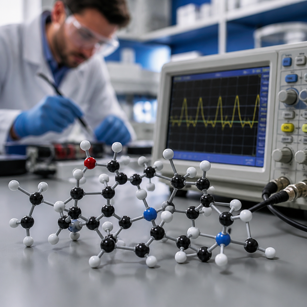
The impact of molecular structure on electrical properties sits at the center of modern materials science because the way atoms are arranged inside a substance determines how easily charge moves, how strongly the material stores electric energy, and how reliably it performs in devices. In practice, when I evaluate a polymer film, ceramic capacitor, conductive coating, or semiconductor layer, I start with structure before I look at any electrical test result. Molecular structure includes bond type, atomic composition, chain length, crystallinity, molecular symmetry, defect density, phase organization, and the interfaces between regions of different order. Electrical properties include conductivity, resistivity, dielectric constant, dielectric loss, breakdown strength, polarization behavior, charge mobility, and frequency response. These properties matter in every sector that depends on electronics: power cables need insulation with high breakdown strength, batteries need controlled ionic transport, integrated circuits need semiconductors with predictable carrier mobility, and sensors need materials whose electrical response changes in measurable ways. A hub article on electrical properties must therefore connect chemistry, physics, processing, and application. The core principle is simple: electrons and ions do not move through an abstract material; they move through a real molecular landscape shaped by bonds, free volume, crystal domains, dipoles, and defects. Change that landscape, and you change performance.
How bonding and electronic structure control conductivity
The first question most readers ask is straightforward: why do some materials conduct electricity while others insulate? The answer begins with electronic structure. In metals, electrons occupy overlapping energy states that allow charge to move freely. In covalent and ionic solids, the gap between filled and empty electronic states can be large, so electrons need significant energy to move. Molecular structure governs that gap. Conjugated systems such as polyaniline, polythiophene, and polyacetylene conduct better than saturated polymers because alternating single and double bonds create delocalized pi electrons. Delocalization lowers the barrier for charge transport. By contrast, polyethylene has strong sigma bonds and no extended conjugation, so it is an excellent insulator.
Bond polarity also matters. In ionic compounds, electrical conduction can occur through ion movement at elevated temperature or in solution, but room-temperature electronic conductivity is usually low unless defects or mixed valence states are present. Transition-metal oxides illustrate this well. Materials such as titanium dioxide, zinc oxide, and indium tin oxide derive useful electrical behavior from crystal chemistry, oxygen vacancies, and dopants that alter carrier concentration. In semiconductor manufacturing, silicon becomes dramatically more conductive when boron or phosphorus atoms are introduced in controlled amounts. That is a structural change at the atomic scale with a large electrical consequence.
From direct lab work with polymer coatings, I have repeatedly seen conductive additives fail when the host matrix isolates them. The chemistry of the backbone may be favorable, but if the structure prevents the formation of percolation pathways, bulk conductivity remains poor. Electrical performance is therefore never just about composition; it is about whether the molecular and mesoscale structure creates a connected path for carriers.
Crystallinity, morphology, and charge transport pathways
Two materials with the same chemical formula can show very different electrical properties if their internal order differs. Crystallinity is a major reason. In semicrystalline polymers, crystalline regions pack chains tightly and can support more efficient transport along ordered segments, while amorphous regions introduce disorder, trap states, and variable hopping distances. The net result depends on the balance between order and connectivity. For example, polyethylene terephthalate and polyvinylidene fluoride can display markedly different dielectric and conduction behavior depending on processing history, cooling rate, orientation, and phase content.
In organic semiconductors, morphology is often the deciding factor for mobility. Regioregular poly(3-hexylthiophene), widely studied in thin-film electronics, performs better when chains align and pi-pi stacking is enhanced. Annealing can improve domain size and ordering, which reduces energetic disorder and facilitates hopping between neighboring sites. The same principle applies in perovskites and small-molecule organic films, where grain boundaries and phase segregation can either assist or obstruct charge extraction.
Defects deserve equal attention. Vacancies, dislocations, chain ends, impurities, and residual solvent create localized states that trap carriers or increase dielectric loss. In ceramic dielectrics such as barium titanate, grain size and grain boundary chemistry strongly affect permittivity and loss tangent. In carbon-filled polymers, dispersion quality controls whether conductive particles form a network or remain electrically isolated. Processing methods such as extrusion, solvent casting, compression molding, and sintering are therefore structural design tools, not mere manufacturing steps.
Key electrical properties and the structural features that drive them
A practical hub page should define the major electrical properties and tie each one to structural causes. Conductivity measures how easily charge moves through a material; resistivity is the inverse and is often used for insulators. Carrier mobility describes how quickly electrons or holes respond to an electric field. Dielectric constant, or relative permittivity, measures how much electric energy a material can store through polarization. Dielectric loss indicates how much of that energy becomes heat. Breakdown strength measures the electric field at which insulation fails. Volume resistivity, surface resistivity, dissipation factor, and polarization relaxation are also important in testing standards such as ASTM and IEC methods.
| Electrical property | Main structural drivers | Representative example |
|---|---|---|
| Conductivity | Conjugation, dopants, percolation pathways, crystal defects | Doped polyaniline in antistatic coatings |
| Carrier mobility | Molecular ordering, pi stacking, grain boundaries, trap density | Annealed organic transistor films |
| Dielectric constant | Permanent dipoles, polarizability, phase composition, ferroelectric domains | PVDF and barium titanate capacitors |
| Dielectric loss | Dipole relaxation, impurities, moisture uptake, interfacial polarization | Humid polymer insulation systems |
| Breakdown strength | Free volume, defects, thickness uniformity, chain packing | Cross-linked polyethylene cable insulation |
Permanent dipoles raise permittivity because aligned molecular units respond to an external field. Fluorinated polymers and nitrile-containing materials often exhibit stronger polarization than nonpolar hydrocarbons. However, higher permittivity can come with greater dielectric loss if dipoles cannot reorient efficiently at the operating frequency. This is one reason structural optimization is always application specific.
Polarization mechanisms, dielectric behavior, and frequency effects
When a material is placed in an electric field, several polarization mechanisms may occur: electronic polarization from displacement of electron clouds, ionic polarization from relative ion movement, dipolar orientation from permanent molecular dipoles, and interfacial polarization from charge accumulation at boundaries. Molecular structure controls all four. Small, highly polarizable atoms contribute differently than rigid dipolar groups. Flexible chains may allow dipoles to reorient, while heavily cross-linked networks may restrict that motion.
Frequency response is essential because a dielectric that performs well at low frequency may lose efficiency at high frequency. In polymers, dipole relaxation times depend on chain mobility, free volume, temperature, and side-group architecture. A classic example is polyvinylidene fluoride, whose polymorphs exhibit different ferroelectric and dielectric behavior because the chain conformations alter net dipole alignment. In ceramic systems, ferroelectric domain dynamics contribute to very high permittivity, but losses can increase near phase transitions.
Moisture is another structural modifier that engineers often underestimate. Water enters free volume, hydrogen-bonds with polar groups, and changes both conductivity and dielectric loss. In epoxy encapsulants and polyamide materials, absorbed moisture can increase leakage current and shift relaxation behavior significantly. During failure analysis, I have traced inconsistent insulation resistance not to formulation errors but to subtle differences in network density and post-cure state that changed moisture uptake.
Polymers, ceramics, composites, and semiconductors in real applications
Different material classes demonstrate the structure-property relationship in distinct ways. In insulating polymers used for wire enamels, films, and cable jackets, long saturated chains, low carrier density, and controlled purity support high resistivity. Cross-linking, as used in cross-linked polyethylene for power cables, improves thermal stability and can enhance resistance to electrical treeing by restricting chain motion. In high-k polymer systems, adding polar groups raises permittivity, but excessive polarity may increase loss and reduce breakdown strength.
Ceramics offer a contrasting model. Barium titanate is valuable in multilayer ceramic capacitors because its crystal structure supports strong polarization and high dielectric constant. Doping and grain-size control tune temperature stability and loss. Alumina, by comparison, is used where reliable electrical insulation and thermal conductivity are both needed. Zinc oxide varistors depend on grain boundary phenomena created during sintering; their nonlinear current-voltage behavior emerges from microstructural barriers rather than simple composition alone.
Composites combine phases to engineer electrical properties. Carbon black, carbon nanotubes, graphene, silver flakes, and metal-coated fibers are added to polymers to create antistatic materials, electromagnetic shielding, or printed conductive traces. The critical concept is the percolation threshold: once filler particles form a connected network, conductivity rises sharply. Filler shape, aspect ratio, surface treatment, and dispersion quality determine how low that threshold can be. In practice, nanotubes can achieve conductivity at lower loading than spherical carbon black, but processing becomes more sensitive and cost often increases.
Semiconductors remain the clearest example of structural control. Crystal orientation, lattice defects, dopant profile, interface quality, and amorphous versus crystalline phase all influence mobility and leakage. Silicon, gallium nitride, silicon carbide, and organic semiconductors each show that atomic arrangement is inseparable from electrical function.
How engineers measure, optimize, and select materials
Electrical property selection should start with the operating environment and failure mode, then work backward to molecular structure. For insulation, key questions include voltage stress, frequency, temperature, humidity, thickness, and expected lifetime. For conductive materials, the priorities may be bulk conductivity, contact resistance, flexibility, and stability under cycling. Standard tools include four-point probe testing for sheet resistance, impedance spectroscopy for frequency-dependent response, dielectric withstand testing, insulation resistance measurement, differential scanning calorimetry for phase behavior, X-ray diffraction for crystallinity, and scanning electron microscopy for morphology.
Optimization usually involves tradeoffs. Increasing crystallinity may improve barrier properties and reduce some forms of conduction, yet excessive crystallinity can create internal stresses or brittleness. Adding conductive filler may reduce resistivity, but it can also raise viscosity, lower elongation, and complicate adhesion. Increasing dipole density may boost dielectric constant, but losses and moisture sensitivity may rise as well. The best material is not the one with the highest number on a datasheet; it is the one whose structure matches the electrical duty cycle over time.
For readers exploring related topics under Materials and Properties, the next logical step is to compare electrical behavior with thermal, mechanical, and barrier properties, because structure couples them all. Molecular design is the bridge. When you understand how bonding, order, defects, interfaces, and processing shape electrical properties, material selection becomes more accurate, troubleshooting becomes faster, and innovation becomes more deliberate. Use this hub as your starting point, then evaluate each material class and test method with structure in mind before making your next design decision.
Frequently Asked Questions
1. How does molecular structure directly affect a material’s electrical properties?
Molecular structure controls electrical behavior because it determines how electrons, ions, and dipoles move through a material. At the most basic level, the types of atoms present, the bonds between them, and the way those atoms are arranged set the energy landscape that charge carriers experience. In conductive materials, a structure that allows electrons to move freely tends to produce higher conductivity. In insulating materials, strongly localized electrons and large energy barriers restrict charge motion. In polar materials, the orientation and mobility of molecular dipoles strongly influence dielectric behavior, including permittivity and energy storage.
When evaluating real materials such as polymer films, ceramic dielectrics, conductive coatings, or semiconductor layers, structure is usually the starting point because it explains why measured electrical performance looks the way it does. Crystallinity, chain alignment, crosslink density, defects, grain boundaries, and phase distribution all matter. A highly ordered structure may support better charge transport in one system, while controlled disorder may be desirable in another if the goal is to suppress leakage current. That is why electrical test data alone rarely tells the full story. The structure determines whether a material behaves as a conductor, semiconductor, dielectric, or insulator, and it also influences stability, reliability, and sensitivity to temperature, frequency, and moisture.
2. Why do bond type and atomic arrangement matter so much in conductivity and insulation?
Bond type and atomic arrangement are central because they define how tightly electrons are held and how easily they can be displaced or transported. In covalent networks, electrons may be strongly shared and localized unless the bonding pattern creates delocalized pathways, as seen in certain conjugated systems. In ionic materials, charge transport may depend less on free electrons and more on ion mobility, which is strongly influenced by lattice structure and available hopping sites. Metallic bonding, by contrast, typically allows a “sea” of mobile electrons, which is why metals conduct so well.
Atomic arrangement adds another level of control. Even if two materials have similar chemical composition, differences in packing, symmetry, and order can produce very different electrical outcomes. For example, a crystal with a regular repeating structure may provide predictable transport pathways, while an amorphous version of the same material may scatter carriers more strongly and show lower conductivity. In dielectric materials, atomic arrangement affects how easily dipoles can align with an applied electric field, which changes permittivity and dielectric loss. This is one reason materials engineers look closely at both chemistry and microstructure: the same atoms can perform very differently depending on how they are organized.
3. How do crystallinity, disorder, and defects influence electrical performance?
Crystallinity, disorder, and defects often determine whether a material performs well or fails in electrical service. In many semiconductors and conductive polymers, greater molecular order can improve carrier mobility by creating more continuous transport pathways. In polymer films, aligned chains and well-developed crystalline regions may help charge move more efficiently along or between molecular segments. In ceramics, a well-controlled crystal structure can improve dielectric response and reduce unwanted losses. However, the relationship is not always simple. More crystallinity does not automatically mean better performance, because interfaces between crystalline and amorphous regions can also trap charge or create localized electric field concentrations.
Defects are equally important. Vacancies, impurities, dislocations, grain boundaries, and chemical irregularities can either help or harm electrical behavior depending on the application. In semiconductors, carefully introduced dopants are essential because they create the desired number of charge carriers. But uncontrolled defects may trap carriers, increase resistance, raise leakage current, or trigger breakdown. In insulating materials, microscopic defects can become the weak points where electrical failure starts. In practical testing, this is why two samples with the same nominal composition may show very different resistivity, dielectric strength, or long-term reliability. Their internal structural quality is different, and the electrical response reveals that difference.
4. What is the connection between molecular structure and dielectric properties such as permittivity and loss?
Dielectric properties depend heavily on how molecular units respond to an electric field. Permittivity reflects how effectively a material can be polarized, and that polarization comes from electronic displacement, ionic movement, dipolar orientation, or interfacial effects. Molecular structure governs all of these mechanisms. If a material contains polar bonds or permanent dipoles that can reorient under an applied field, it may show higher permittivity. If its structure restricts that motion, the dielectric response may be lower but more stable. Flexible polar groups, backbone architecture, side-chain design, and intermolecular spacing all contribute to how the material stores electric energy.
Dielectric loss is just as important, especially in capacitors, coatings, and high-frequency electronics. A structure that allows excessive dipole lag, charge hopping, or interfacial polarization can waste energy as heat. Moisture absorption, impurities, and structural heterogeneity often increase dielectric loss because they introduce additional polarization and conduction pathways. In polymer and ceramic design, the goal is often to balance high permittivity with low loss and strong breakdown resistance. That balance is structural in nature. Engineers tune composition, phase content, chain mobility, and interface quality to achieve the required electrical response across operating frequencies and temperatures.
5. How is molecular structure used to design better electrical materials for real-world devices?
In real-world materials development, molecular structure is the main design lever used to tailor performance for a specific electrical function. If the target is higher conductivity, researchers may introduce conjugated pathways, conductive fillers, or dopants that create more efficient charge transport networks. If the goal is insulation, they may increase bond strength, reduce free volume, limit mobile charge carriers, and suppress defect formation. For dielectric applications, they may engineer polar groups, crystalline phases, or composite interfaces to raise energy storage capability without causing excessive leakage or dielectric loss.
This structural approach is used across industries. In polymer electronics, chain architecture and orientation affect flexibility, conductivity, and environmental stability. In ceramic capacitors, crystal chemistry and grain boundary engineering control permittivity, temperature dependence, and breakdown strength. In semiconductors, band structure and defect control define switching behavior and carrier mobility. In coatings and films, morphology and dispersion quality determine whether the final layer acts as a barrier, static dissipative surface, or conductive path. The reason structure comes first in evaluation is simple: once you understand how atoms and molecules are arranged, you can make sense of the electrical data and predict how the material will behave in service over time.