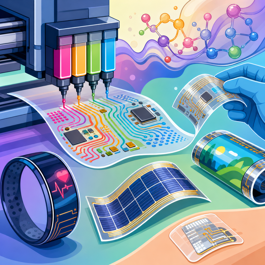
Printed electronics has moved from a niche manufacturing concept to a practical platform for sensors, displays, medical patches, smart packaging, and flexible circuits, and polymers are the materials making that transition possible. In this field, electronic functionality is created through printing methods such as inkjet, screen, gravure, and flexographic printing rather than by relying only on conventional subtractive semiconductor fabrication. Polymers matter because they appear at every layer of the stack: as substrates, dielectric films, semiconducting channels, conductive binders, encapsulants, and stretchable adhesives. After working with formulation teams and device engineers on pilot lines, I have seen the same pattern repeatedly: when a printed electronic product succeeds commercially, it is usually because polymer selection was treated as a device architecture decision, not a packaging afterthought.
The term polymer covers a broad class of materials made from repeating molecular units, but in printed electronics the distinction between commodity plastics and functional polymers is critical. Polyethylene terephthalate, polyethylene naphthalate, and polyimide are widely used as substrate films because they combine smooth surfaces, roll-to-roll processability, and useful thermal stability. Conductive polymers such as PEDOT:PSS can replace brittle transparent conductors in some applications. Semiconducting polymers based on donor-acceptor backbones can transport charge in printed transistors. Elastomers like TPU and silicone enable stretchable circuits that survive bending and skin movement. In practical terms, polymers give designers tunable mechanical, optical, electrical, and barrier properties at lower process temperatures than silicon wafers or glass usually require.
This matters because the electronics industry is being pushed toward lighter form factors, larger areas, lower capital intensity, and new use cases that rigid boards cannot address economically. A disposable biosensor patch does not need the same architecture as a smartphone logic chip, but it does need manufacturability at scale, comfort, reliability, and low cost. A smart label for cold-chain monitoring must survive logistics handling, print at high throughput, and communicate clearly with readers or users. Polymers make those combinations achievable. They support roll-to-roll manufacturing, compatibility with additive deposition, and integration onto paper, film, textiles, and curved surfaces. For the broader applications landscape, electronics is the hub because advances here influence healthcare wearables, automotive interiors, retail packaging, industrial sensing, and energy systems simultaneously.
Why polymers are foundational to printed electronics
Polymers are revolutionizing printed electronics because they solve the central mismatch between traditional electronic materials and emerging product requirements. Silicon, indium tin oxide, and vacuum-deposited metals deliver high performance, but they are often rigid, brittle, expensive to process over large areas, or poorly suited to low-temperature substrates. Polymer-based systems can be engineered for flexibility, adhesion, rheology, solvent compatibility, and environmental resistance. In manufacturing, those properties are not secondary. Ink viscosity determines whether a nozzle jets cleanly. Surface energy controls wetting and line definition. Glass transition temperature limits curing conditions. Oxygen and moisture permeability influence shelf life and device drift. Polymer design lets engineers tune those variables intentionally.
One of the clearest examples is the shift from rigid printed circuit assumptions to mechanically compliant devices. When I evaluate failure reports from flexible prototypes, cracking rarely begins with the active material alone; it often starts at an interface where modulus, adhesion, and strain distribution were not balanced. A polymer interlayer can absorb stress, improve adhesion, and preserve conductivity during repeated bending. This is why polymer science sits at the center of flexible hybrid electronics, where printed traces, mounted components, adhesives, and barrier layers all need matched mechanical behavior. It is also why device performance cannot be judged only by initial conductivity or mobility. A printed sensor that works on day one but drifts after sweat exposure, UV exposure, or 10,000 flex cycles is not commercially viable.
Polymers also support additive manufacturing economics. Traditional microelectronics relies heavily on photolithography, etching, and vacuum systems, all of which can deliver exceptional precision but with high capital cost and material waste. Printed electronics uses patterned deposition, often in ambient or near-ambient environments, to place material only where needed. Polymer inks and coatings are central to that approach because they can carry functional particles, stabilize dispersions, control drying, and form uniform films on fast-moving webs. For many applications, especially large-area and disposable electronics, that process advantage is more important than chasing the highest possible transistor speed.
Key polymer classes used in electronic applications
Several polymer families dominate commercial and developmental printed electronics. Substrate polymers include PET, valued for low cost and optical clarity; PEN, which offers better thermal resistance and dimensional stability than PET; and polyimide, preferred when processing temperatures are higher or long-term heat resistance matters. For stretchable systems, thermoplastic polyurethane, styrene-ethylene-butylene-styrene, and silicones are common because they tolerate large strains. Encapsulation films may use fluoropolymers, epoxy systems, or multilayer barrier laminates depending on whether flexibility, moisture resistance, or chemical durability is the top priority.
Functional polymers add the electronic behavior. PEDOT:PSS remains the best-known conductive polymer, used in antistatic layers, electrodes, biointerfaces, and some transparent conductive films. Its conductivity can be improved through secondary doping and post-treatment with solvents such as DMSO or ethylene glycol, though those changes can affect stability and printability. Semiconducting polymers include materials derived from polythiophenes and donor-acceptor systems such as diketopyrrolopyrrole-based backbones. These are used in organic thin-film transistors and photodetectors because their molecular structure can be tailored to influence charge mobility, bandgap, and morphology. Dielectric polymers such as crosslinked PMMA, PVP systems, and fluorinated materials are used to insulate layers and shape transistor operation.
| Polymer type | Common examples | Primary role in printed electronics | Typical advantage |
|---|---|---|---|
| Substrate polymers | PET, PEN, polyimide | Mechanical support for printed layers | Flexible, lightweight, roll-to-roll compatible |
| Conductive polymers | PEDOT:PSS | Electrodes, antistatic films, biointerfaces | Transparent, flexible, solution processable |
| Semiconducting polymers | P3HT, DPP-based polymers | Transistor channels, photodetectors | Tunable electronic properties |
| Dielectric polymers | PMMA, PVP, fluorinated dielectrics | Insulation and gate dielectric layers | Low-temperature film formation |
| Elastomeric polymers | TPU, silicone, SEBS | Stretchable circuits and wearables | High strain tolerance |
These categories often overlap in real products. A wearable patch may combine a TPU substrate, a silver-flake ink with polymer binder, a PEDOT:PSS electrode at the skin interface, an acrylic adhesive, and a polyurethane barrier topcoat. The final device behavior depends on the entire polymer system, not just one celebrated active layer. That systems view is essential for anyone using this electronics hub to explore connected topics such as sensors, medical devices, displays, or smart packaging.
How polymers enable modern manufacturing methods
Printing processes impose strict demands that polymers are uniquely suited to meet. In inkjet printing, formulations need controlled viscosity, surface tension, particle size, and drying behavior to avoid nozzle clogging and coffee-ring defects. Polymeric dispersants and binders stabilize inks and help printed features retain shape after deposition. In screen printing, higher-viscosity pastes depend on polymer rheology modifiers to pass through the mesh cleanly and recover enough body to preserve fine patterns. Gravure and flexographic lines, which are attractive for high-volume production, rely on fast-drying formulations and substrate surfaces engineered for uniform transfer.
Roll-to-roll processing is where polymers show their industrial value most clearly. Web tension, thermal expansion, solvent exposure, and registration accuracy all interact with substrate choice. PET may be sufficient for low-temperature conductive traces and labels, while PEN or polyimide may be necessary when curing temperatures increase or multilayer alignment becomes more demanding. Corona treatment, plasma treatment, and primer coatings are frequently used to modify polymer film surfaces so inks wet consistently. Without that surface engineering, even a well-designed conductive ink can bead, dewet, or spread unpredictably, producing open circuits or variable resistance.
Curing and sintering strategies are also shaped by polymers. Metallic inks often require heat to drive off solvents and fuse particles, but polymer substrates can only tolerate limited temperature. That constraint has accelerated the use of photonic curing, chemical sintering, low-temperature nanoparticle systems, and hybrid inks where polymer matrices maintain conductivity with reduced thermal budgets. In production environments, the winning process is rarely the one with the best lab conductivity. It is the one that delivers acceptable conductivity, dimensional stability, and yield at line speed on the target substrate.
Real-world applications transforming the electronics market
Flexible displays and touch interfaces are one visible example of polymers changing electronics. Polymer films reduce breakage risk compared with glass and support curved or foldable designs. While premium displays still rely on sophisticated multilayer stacks, polymer substrates and barrier layers are fundamental to making these architectures thin and mechanically durable. In automotive interiors, printed capacitive touch controls on molded plastic surfaces are replacing bulky switch assemblies. The benefit is not only aesthetics; printed polymer-based electronics reduce part count, simplify assembly, and allow controls to conform to complex shapes.
Wearable and medical electronics show an even stronger polymer advantage. Skin-mounted ECG, hydration, temperature, and electrophysiology patches must flex with the body, maintain signal quality, and remain comfortable for hours or days. Conductive polymers and elastomeric substrates help match the mechanical softness of skin better than rigid electrodes can. In commercial biosensing, printed glucose and lactate strips have long demonstrated the value of scalable printing, and newer continuous monitoring patches are extending that model with flexible interconnects and soft encapsulation. Regulatory requirements remain stringent, but polymer-based device architectures are helping manufacturers reduce irritation, improve adhesion, and support disposable formats.
Smart packaging and item-level sensing are another major growth area. Near-field communication tags, temperature indicators, and printed battery-assisted labels can be integrated into cartons, pouches, or labels using polymer films and coatings. The economics work because additive printing reduces waste and supports high-throughput production over large areas. For logistics and cold-chain monitoring, the combination of a polymer substrate, printed antenna, sensor element, and simple display or memory can deliver actionable data without the cost structure of conventional electronics assembly. Retailers, pharmaceutical distributors, and food producers increasingly view these systems as operational tools rather than experimental novelties.
Performance limits, reliability challenges, and design tradeoffs
Polymers are enabling printed electronics, but they also introduce constraints that engineers must manage carefully. Charge mobility in polymer semiconductors is lower than in crystalline silicon, so they are not replacing high-performance computing devices. Oxygen and moisture sensitivity can degrade organic materials, making encapsulation essential. Conductive polymers may suffer from environmental drift, especially when exposed to humidity or repeated washing. Polymer substrates can creep, shrink, or warp under heat, compromising registration and multilayer alignment. These are not minor details; they define whether a product can scale beyond a pilot line.
Reliability testing has to reflect the actual use case. For wearable electronics, I look for bending radius tests, cyclic strain data, sweat exposure, adhesive aging, and electrical stability after laundering or sterilization when relevant. For packaging electronics, abrasion, drop events, temperature cycling, and warehouse humidity may matter more than extreme flex life. Standards from IPC, ASTM, and ISO help, but many printed electronics products still require application-specific qualification plans because the failure modes differ from those of rigid boards. A silver trace on TPU fails differently from a copper trace on FR-4, and the test methodology needs to acknowledge that reality.
There are also sustainability tradeoffs. Polymers can reduce material waste through additive processing and support lower-energy manufacturing, yet multilayer constructions may complicate recycling. Solvent systems, fluorinated chemistries, and mixed-material laminates require scrutiny. The strongest development programs now consider disassembly, solvent selection, and mono-material strategies earlier in design. That is especially important for disposable electronics, where the environmental case must be as convincing as the technical one.
What comes next for polymer-based printed electronics
The next phase of growth will come from better materials integration, not from one breakthrough polymer replacing all others. Hybrid systems that combine printed polymers with silicon chips, thin sensors, or conventional components are already delivering practical products. This approach, often called flexible hybrid electronics, uses each material where it performs best: silicon for computation, printed polymers for large-area interconnects, sensing surfaces, or conformal form factors. As manufacturing lines mature, expect tighter process control, more standardized qualification methods, and broader use in automotive, healthcare, consumer devices, and industrial monitoring.
Materials science is also moving toward higher stability and more sustainable formulations. Researchers are improving semiconducting polymer morphology control, stretchable conductor networks, self-healing elastomers, and barrier coatings with lower defect density. At the same time, manufacturers are pushing water-based inks, lower-temperature curing, and recyclable substrate options where application requirements allow. Those incremental advances matter because printed electronics succeeds through manufacturable combinations, not isolated record-setting data. For companies evaluating adoption, the key question is simple: where do polymer-enabled form factor, weight, cost, or manufacturing advantages create a product that rigid electronics cannot match efficiently?
Polymers are revolutionizing printed electronics by turning electronics into something that can be printed, bent, stretched, laminated, and integrated into everyday objects at industrial scale. They provide the substrate, functionality, and process control needed for sensors, wearables, smart labels, displays, and conformal interfaces. Just as important, they allow manufacturers to tailor mechanical behavior, thermal budgets, and surface interactions in ways conventional materials often cannot. The result is not a replacement for all silicon electronics, but a powerful expansion of what electronics can be and where it can go.
For anyone building an applications strategy around electronics, polymer-based printed systems deserve close attention because this is the platform connecting product design with scalable manufacturing. The most successful teams treat polymer choice as a core engineering decision, validate reliability under real conditions, and align material selection with end-of-life considerations from the start. Use this hub as the starting point for deeper exploration of sensors, medical devices, displays, smart packaging, and flexible hybrid systems, then map those technologies against your own performance and cost targets. That is where practical adoption begins.
Frequently Asked Questions
1. Why are polymers so important in printed electronics?
Polymers are central to printed electronics because they contribute to nearly every functional and structural layer in a printed device. They are used as substrates, binders, dielectric layers, encapsulants, adhesives, and, in many cases, as active electronic materials themselves. This broad role is what makes them so valuable. Instead of depending only on rigid, high-temperature, subtractive manufacturing methods used in conventional semiconductor production, printed electronics relies on depositing materials in patterned layers through processes such as inkjet, screen, gravure, and flexographic printing. For those methods to work at scale, the materials must flow well, cure under practical conditions, adhere to the right surfaces, and maintain performance during bending, rolling, or stretching. Polymers are exceptionally good at meeting those requirements.
Another reason polymers matter is tunability. Their chemistry can be adjusted to optimize viscosity, surface energy, conductivity support, flexibility, thermal stability, barrier performance, and compatibility with different printing systems. That allows manufacturers to design formulations for specific applications, whether the goal is a disposable smart label, a flexible display component, a wearable medical patch, or a lightweight sensor array. In practical terms, polymers are helping move printed electronics from laboratory demonstrations into real products because they make devices easier to print, more mechanically durable, and more compatible with low-cost, high-throughput manufacturing.
2. How do polymers improve the performance and manufacturability of printed electronic devices?
Polymers improve both performance and manufacturability by acting as enablers at the material-process interface. In printed electronics, it is not enough for a material to have useful electrical properties; it also has to behave predictably during deposition, drying, curing, and long-term use. Polymers help solve that challenge. As binders in conductive or functional inks, they control rheology, stabilize dispersed particles, promote adhesion, and support line definition during printing. That means better print uniformity, fewer defects, and more reliable device performance across large production volumes.
On the performance side, polymers are especially important in applications where flexibility is a requirement rather than a convenience. Traditional electronic materials often perform well electrically but are brittle or difficult to process on thin, bendable films. Polymers allow electronic layers to survive repeated flexing, folding, or conformal mounting on curved surfaces. They also serve as dielectric layers in capacitors and transistors, protective encapsulation against moisture and oxygen, and interface layers that improve device stability. In wearable and medical applications, polymer materials can be chosen for softness, breathability, and even skin compatibility. In smart packaging, they can support low-cost printing on large areas while maintaining enough durability for shipping and handling. Altogether, polymers reduce manufacturing complexity while improving reliability, mechanical resilience, and integration into nontraditional form factors.
3. What types of polymers are commonly used in printed electronics?
Printed electronics uses a wide range of polymers, and the specific choice depends on whether the polymer is serving a structural, insulating, protective, or electronic role. For substrates, common polymer films include polyethylene terephthalate (PET), polyethylene naphthalate (PEN), and polyimide. PET is widely used because it is cost-effective, flexible, and suitable for many large-area printed applications. PEN offers improved thermal and dimensional stability, while polyimide is chosen when higher processing temperatures or more demanding environments are involved.
In ink formulations, polymers may function as binders or dispersants that help conductive particles or functional additives print consistently. Dielectric polymers are used to create insulating layers, gate dielectrics, and separator structures in printed components. Encapsulation polymers protect sensitive layers from moisture, oxygen, abrasion, and chemical exposure. There are also intrinsically conductive polymers, such as PEDOT:PSS, that can serve as transparent conductors, electrode materials, or hole transport layers depending on the device design. Semiconducting polymers are another important category, particularly in organic transistors, printed sensors, and emerging display and photovoltaic technologies. What makes this material family so powerful is that it spans passive support roles and active electronic roles, allowing engineers to build multilayer devices with materials that are compatible with the same general printing ecosystem.
4. Which applications are benefiting most from polymer-enabled printed electronics?
A wide variety of industries are benefiting, especially those that need electronics to be lightweight, flexible, low-cost, and scalable over large areas. Sensors are one of the biggest success stories. Printed sensor platforms for temperature, humidity, pressure, strain, gas detection, and biosensing often depend on polymer substrates and polymer-based inks to deliver flexibility and manufacturing efficiency. These are increasingly used in industrial monitoring, consumer products, agriculture, and healthcare.
Wearable medical patches are another major area of growth. Polymers make it possible to create soft, thin electronic systems that can conform to skin, support signal collection, and remain comfortable over extended use. In displays and lighting, polymer materials support flexible form factors and can act as key layers in printed organic electronic architectures. Smart packaging also benefits significantly because polymer-compatible printing methods can add connectivity, sensing, authentication, or freshness monitoring features directly onto labels and cartons at commercially relevant speeds. Flexible circuits, RFID tags, disposable diagnostics, and human-machine interfaces are also advancing rapidly because polymer materials make these products more adaptable and economically viable. The common thread across all these applications is that polymers enable electronic functionality to be integrated into places where rigid silicon-based assemblies would be too expensive, too bulky, or too mechanically limiting.
5. What are the biggest challenges and future opportunities for polymers in printed electronics?
Despite major progress, there are still important challenges. One of the biggest is balancing printability, electrical performance, durability, and cost in a single material system. A polymer that prints beautifully may not always deliver the best long-term environmental stability, and a material with excellent electronic properties may require processing conditions that are difficult to scale on low-cost flexible substrates. Moisture sensitivity, oxygen exposure, thermal limitations, interlayer adhesion, and batch-to-batch consistency remain active areas of development. Device lifetime is especially important for products that must operate reliably in real-world conditions, including wearables, outdoor sensors, and supply-chain packaging.
That said, the future opportunities are substantial. Material innovation is expanding toward polymers with improved conductivity support, better barrier performance, higher stretchability, and greater compatibility with sustainable manufacturing. Researchers and manufacturers are also working on recyclable substrates, lower-temperature curing systems, solvent systems with improved environmental profiles, and multifunctional polymers that combine mechanical and electronic roles in fewer layers. As printing equipment, process control, and material science continue to mature together, polymers are expected to play an even larger role in bringing electronics into everyday objects. That includes smarter packaging, more accessible point-of-care diagnostics, flexible energy devices, interactive surfaces, and next-generation wearable systems. In short, polymers are not just supporting the evolution of printed electronics; they are one of the main reasons the field is becoming commercially practical and technologically transformative.