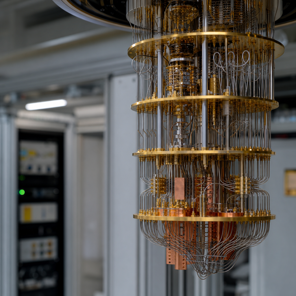
Quantum computing depends on exquisitely controlled materials, and polymers are becoming essential to how those materials are packaged, patterned, insulated, stabilized, and scaled. In this subtopic hub for polymers in high-tech and electronics, the central question is straightforward: how can soft, chain-based materials support devices built on some of the most delicate physical phenomena ever engineered? The answer is broader than many readers expect. Polymers already influence semiconductor fabrication, advanced lithography, flexible circuitry, cryogenic insulation, dielectric performance, electromagnetic shielding, encapsulation, and photonic integration, all of which intersect with practical quantum hardware development.
A polymer is a material made of repeating molecular units, natural or synthetic, that can be engineered for mechanical strength, chemical resistance, dielectric behavior, thermal stability, optical clarity, or nanoscale patternability. Quantum computing, by contrast, uses quantum states such as superposition and entanglement to perform certain calculations more efficiently than classical systems. Today’s leading hardware platforms include superconducting circuits, trapped ions, silicon spin qubits, neutral atoms, and photonic systems. Each platform has different bottlenecks, yet all require precise material stacks, contamination control, low-loss interfaces, and manufacturable packaging. That is where polymers enter the picture.
In my work reviewing electronics materials programs, I have seen polymers dismissed as secondary because they are rarely the active qubit medium. That view misses how real systems are built. A quantum processor is not just a qubit chip. It is a layered assembly of substrates, interposers, adhesives, coatings, cable dielectrics, photoresists, underfills, thermal interface structures, and shielding components that must survive fabrication and often operate at cryogenic temperatures. If any of those support materials introduce mechanical stress, outgassing, dielectric loss, moisture ingress, or particle contamination, qubit coherence and device yield can suffer.
This matters because the industry is moving from laboratory demonstrations toward manufacturable, repeatable systems. Researchers can hand-build a few devices with heroic process control, but useful quantum computing requires consistency across many chips, modules, and cooling cycles. Polymers help close that gap by enabling reproducible lithographic patterning, low-mass cable insulation, compact packaging, wafer-level processing, and hybrid integration with classical control electronics. For readers exploring case studies and applications, this article serves as the hub for polymers in high-tech and electronics by showing where polymers add value, where they create risk, and which material decisions shape quantum performance most directly.
Why polymers matter in quantum hardware
Polymers support quantum computing primarily as enabling materials rather than qubit materials. Their most important roles include photoresists for nanoscale patterning, dielectric layers for insulation, encapsulants for device protection, flexible substrates for interconnects, and cable jackets for cryogenic wiring. In superconducting quantum processors, for example, even a tiny dielectric loss tangent in nearby materials can contribute to decoherence. That means engineers do not simply ask whether a polymer survives processing; they ask whether it remains electrically quiet, mechanically stable, and chemically clean under vacuum and at millikelvin or low-kelvin conditions.
One practical example comes from lithography. Many quantum devices use electron-beam or deep ultraviolet lithography to define Josephson junctions, resonators, waveguides, or fine interconnects. Poly(methyl methacrylate), commonly called PMMA, is a standard electron-beam resist because it offers predictable resolution and process behavior. SU-8, an epoxy-based negative resist, appears in microfluidic and MEMS-adjacent fabrication where tall structures are needed. Polyimide is widely used in advanced electronics for flexible circuits and stress-buffering layers because it resists heat better than many commodity plastics. These materials do not compute, but they make the device architecture manufacturable.
Polymers also matter because they help reconcile conflicting engineering demands. Quantum hardware often needs low thermal conductivity to reduce heat leaks, but also dimensional stability during cooldown. It needs electrical insulation, but not excessive dielectric participation. It needs strong adhesion, but minimal contamination. High-performance polymers such as PEEK, PTFE, polyimide, LCP, parylene, and benzocyclobutene are considered because each offers a different balance of thermal, mechanical, and electrical properties. Material selection is therefore system-specific, and that selection process is one of the most important themes in polymers in high-tech and electronics.
Key polymer functions across fabrication, packaging, and operation
To understand how polymers support quantum computing, it helps to map their roles across the hardware lifecycle. In fabrication, polymers appear as resists, planarization layers, transfer media, sacrificial layers, and contamination barriers. In packaging, they become underfills, adhesives, wire coatings, strain reliefs, sealants, and multilayer circuit dielectrics. During operation, especially in cryogenic environments, they can provide insulation, reduce vibration transfer, and protect components from moisture or handling damage. The same polymer can be useful in one stage and problematic in another, which is why process integration matters more than catalog specifications.
| Polymer or class | Common quantum-relevant use | Main advantage | Main concern |
|---|---|---|---|
| PMMA | Electron-beam resist | High-resolution patterning | Residue after lift-off or development |
| Polyimide | Flexible circuits, insulation, stress buffer | High thermal stability | Moisture uptake and dielectric loss must be managed |
| PTFE | Cable dielectric, insulation | Low dielectric constant and chemical inertness | Mechanical creep and joining difficulty |
| Parylene | Conformal coating | Uniform thin-film coverage | Adhesion and trapped contamination risks |
| BCB | Low-k dielectric, wafer bonding | Low dielectric loss and good planarization | Process sensitivity during curing |
| LCP | High-frequency flexible substrates | Low moisture absorption | Fabrication ecosystem is narrower than polyimide |
That balance is visible in cryogenic cable assemblies. PTFE and related fluoropolymers are widely used because they combine electrical insulation with good high-frequency performance and low outgassing. However, their mechanical behavior under repeated thermal cycling can create design constraints at connectors and bends. Engineers often add strain relief, tune bend radius, and qualify assemblies through multiple cooldown cycles. In quantum systems, those reliability details are not peripheral. A failing cable or drifting dielectric changes the measurement chain and can cost weeks of experimental time.
Polymers in superconducting, photonic, and spin-based platforms
Different quantum platforms use polymers differently. Superconducting systems, the most commercially visible today, are especially sensitive to dielectric loss and two-level system defects at interfaces. For these devices, polymer exposure near resonators or junctions is minimized after patterning, and cleaning protocols are tightly controlled. Residual resist left from PMMA or other lithographic materials can degrade microwave performance. Teams often use oxygen plasma descum, solvent optimization, or downstream ash processes to reduce organic residue, then verify surfaces with ellipsometry, XPS, or contact-angle measurements.
Photonic quantum computing creates a different opportunity set. Polymer waveguides, polymer claddings, UV-curable adhesives, and alignment structures can simplify the assembly of optical components. In integrated photonics, polymers can provide low-cost routing or packaging around silicon nitride or silicon photonic circuits. They may also enable tunability through thermo-optic effects. The tradeoff is that optical loss, long-term aging, and thermal drift must be characterized carefully. For chip-to-fiber coupling, a polymer adhesive with the wrong coefficient of thermal expansion can misalign components during temperature changes and reduce photon collection efficiency.
Silicon spin qubits and related semiconductor approaches also depend on polymer-enabled processing. Advanced patterning, wafer bonding, temporary handling layers, and redistribution structures frequently use polymer materials. In heterogeneous integration, where quantum chips are brought closer to classical control or readout circuitry, polymer dielectrics and underfills help manage mechanical stress and routing density. The challenge is to preserve low-noise electrical behavior while maintaining yield. In practice, this means selecting formulations with low ionic contamination, qualifying cure schedules, and measuring whether a polymer changes charge noise or trap density near active regions.
Cryogenic performance, dielectric loss, and contamination control
The most important technical issue for polymers in quantum computing is not simply whether they work at low temperature. It is whether they remain benign when every source of loss, noise, and stress matters. At cryogenic temperatures, polymers can shrink differently from metals, ceramics, and semiconductors, creating interfacial stress. Some become brittle. Others trap absorbed moisture or release trace volatiles during pump-down. In microwave quantum hardware, dielectric loss and parasitic coupling are central concerns, which is why engineers care about dissipation factor, relative permittivity, and field participation ratios instead of only bulk mechanical data.
Contamination control is equally decisive. Organic residues can remain after lithography, bonding, handling, or packaging, and those residues may alter surface chemistry in ways that hurt coherence or reliability. Fabrication teams address this by limiting polymer residence time, using filtered chemistries, validating bake conditions, and choosing materials with known low-outgassing behavior. NASA outgassing databases, IPC cleanliness practices, and semiconductor contamination protocols are useful references, even though quantum hardware imposes tighter performance sensitivity than many conventional electronics applications.
I have repeatedly seen teams improve device consistency not by changing the qubit design first, but by tightening polymer process discipline: fresher resist, cleaner lift-off, better solvent exchange, lower-residue masking, and stricter incoming material control. Those changes do not sound glamorous, yet they often affect yield faster than more ambitious architecture changes. That is why any serious discussion of how polymers support the development of quantum computing must include process hygiene, not just material names.
Case studies from the broader high-tech and electronics ecosystem
Quantum computing benefits from lessons already learned in adjacent industries. Semiconductor packaging offers a clear example. Polyimide redistribution layers, epoxy underfills, and low-k dielectrics have been optimized for decades to handle fine-pitch routing, thermal excursions, and reliability testing. Not all of those materials transfer directly into cryogenic quantum systems, but the screening methods do. Engineers use thermal cycling, shear testing, dielectric characterization, and failure analysis to identify formulations that maintain adhesion and electrical integrity.
Another instructive case is aerospace electronics, where low outgassing, radiation tolerance, and thermal stability are critical. Materials such as PEEK, PTFE, and parylene were adopted because standard plastics could not survive the environment or cleanliness requirements. Quantum hardware shares a similar intolerance for uncontrolled contamination and thermal mismatch, especially inside dilution refrigerators and vacuum enclosures. Medical devices and advanced sensors offer a third parallel: conformal coatings and flexible polymer circuits enable compact, reliable integration where rigid assemblies would fail mechanically.
These examples explain why this hub topic extends beyond quantum alone. Polymers in high-tech and electronics include 5G antennas, flexible displays, semiconductor lithography, photonic packaging, battery insulation, and high-frequency interconnects. Quantum computing sits within that broader materials ecosystem. The companies and research groups that progress fastest usually borrow proven polymer characterization methods from these neighboring sectors instead of treating quantum as a completely isolated domain.
What comes next for polymer-enabled quantum systems
The next phase of quantum hardware development will demand polymers with lower dielectric loss, better cryogenic property data, cleaner processing windows, and tighter lot-to-lot consistency. Suppliers that can document ionic purity, volatile content, cure behavior, coefficient of thermal expansion, and microwave performance at low temperature will have a real advantage. There is also growing interest in polymer composites loaded with thermally conductive but electrically insulating fillers, ultra-low-loss photo-patternable dielectrics, and recyclable materials for cleaner fabrication workflows.
Machine learning for materials selection may help identify polymer formulations that reduce stress and contamination simultaneously, but experimental validation will remain essential. Quantum devices are unusually sensitive to interfaces, and interface behavior cannot be inferred reliably from room-temperature bulk data alone. That is why future progress will come from coordinated testing across chemistry, processing, packaging, and device physics. The best teams already run these loops together.
Polymers support the development of quantum computing by making fragile hardware manufacturable, connectable, and operable in the real world. They define patterns, insulate lines, protect assemblies, and enable integration across chips, cables, and photonic components. They also introduce real risks when dielectric loss, residue, moisture, or thermal mismatch are ignored. For anyone building knowledge in case studies and applications, the main takeaway is clear: polymer choices are design choices in advanced electronics. Explore the linked subtopics under polymers in high-tech and electronics, compare material-performance tradeoffs carefully, and use this hub as the starting point for deeper evaluation of fabrication, packaging, and reliability strategies.
Frequently Asked Questions
1. Why are polymers important in the development of quantum computing?
Polymers matter in quantum computing because they help solve many of the practical engineering problems that sit between a laboratory qubit and a usable quantum device. Quantum systems are extremely sensitive to heat, vibration, electrical noise, chemical contamination, and mechanical stress. Polymers are valuable because they can be engineered to act as insulators, protective coatings, structural supports, dielectric layers, photoresists, encapsulants, adhesives, and interface materials, all while being processed with high precision and at scale.
In many quantum hardware platforms, including superconducting circuits, spin qubits, photonic quantum devices, and advanced semiconductor architectures, the challenge is not just creating the active quantum element. It is also building the surrounding environment so that the qubit remains stable and controllable. Polymers contribute by enabling fine patterning during fabrication, protecting delicate surfaces from damage, reducing unwanted interactions between components, and supporting advanced packaging strategies that keep device geometries consistent.
They are also important from a manufacturing perspective. Many polymer-based materials are already deeply integrated into microelectronics production, so researchers can adapt existing lithography, coating, and packaging methods for quantum applications. That makes polymers especially attractive for scaling quantum technologies beyond one-off prototypes. In other words, polymers may not always be the material hosting the quantum state itself, but they are often essential to making the full device manufacturable, reliable, and practical.
2. How do polymers help protect delicate quantum devices from environmental interference?
Environmental interference is one of the biggest obstacles in quantum computing, and polymers help address it in several complementary ways. Quantum devices can lose coherence when exposed to thermal fluctuations, electromagnetic disturbances, moisture, oxygen, surface contamination, or mechanical strain. Carefully selected polymers can serve as barrier layers, insulating films, low-stress coatings, and encapsulation materials that shield sensitive structures from these outside influences.
For example, polymer coatings can protect surfaces during fabrication and operation by limiting exposure to dust, reactive chemicals, and humidity. In packaging, polymer-based materials can be used to reduce mechanical damage and provide controlled spacing between components. Flexible polymer interlayers can also help absorb or redistribute stress that might otherwise crack brittle substrates or disturb highly tuned device architectures. This is especially useful when different materials with different thermal expansion behaviors are assembled together and then cooled to very low temperatures.
Another major role is electrical isolation. Quantum hardware often includes densely packed circuitry, control lines, and support electronics, all of which must be separated to prevent parasitic coupling and signal loss. Polymer dielectrics can help isolate these structures while maintaining precise layouts. That said, not every polymer is suitable. At quantum-relevant temperatures and frequencies, material impurities, dielectric loss, and outgassing become critical concerns. So the value of polymers lies not just in using them, but in choosing or designing formulations that introduce as little noise and instability as possible.
3. Are polymers used directly in quantum chips, or mainly in fabrication and packaging?
The answer is both, although their most established role today is in fabrication, integration, and packaging rather than as the primary quantum-active medium. In the fabrication stage, polymers are widely used as photoresists and electron-beam resists to define nanometer- and micrometer-scale patterns. These patterning materials are fundamental to creating the electrodes, waveguides, junctions, cavities, and other microstructures that quantum devices require. Without polymer-based resist systems, it would be much harder to manufacture the intricate layouts seen in modern quantum hardware.
Polymers also appear in dielectric layers, planarization coatings, adhesives, membranes, flexible supports, and encapsulation systems. In advanced chip packaging, they can help connect quantum chips to control hardware, maintain alignment, manage stress, and electrically isolate neighboring structures. These functions are crucial because quantum performance depends heavily on the integrity of the full device stack, not just the qubit element itself.
In some emerging areas, polymers may play more direct roles. Researchers are exploring polymer-containing composites, polymer-derived interfaces, organic and hybrid electronic materials, and specialty molecular systems that could influence charge transport, spin behavior, or photonic routing. There is also interest in polymer-based materials for flexible quantum sensors and supporting optoelectronic elements used alongside quantum circuits. Still, most near-term quantum platforms rely on polymers primarily as enabling materials around the qubit, where their tunability and processing advantages can be used without compromising the fragile physics at the core of the device.
4. What properties make a polymer suitable for quantum computing applications?
A polymer intended for quantum computing must satisfy a much stricter set of requirements than one used in ordinary electronics. First, it needs excellent chemical purity. Even tiny amounts of residual solvents, ions, moisture, or molecular contaminants can affect the surfaces and interfaces that quantum devices depend on. Low outgassing is also essential, especially in vacuum environments or cryogenic systems where volatile species can condense onto sensitive components and degrade performance.
Second, electrical behavior matters enormously. Many quantum systems require low dielectric loss, stable insulation, and minimal charge trapping. If a polymer stores charge unpredictably or couples too strongly to electromagnetic fields, it can introduce noise and reduce qubit coherence. Thermal behavior is equally important. Quantum hardware often operates at extremely low temperatures, so polymers must maintain dimensional stability, avoid cracking, and behave predictably during repeated cooling and warming cycles. A mismatch in thermal expansion between a polymer and neighboring materials can create strain that disturbs delicate device features.
Mechanical and processing properties are also critical. The material may need to form uniform thin films, support high-resolution lithography, bond reliably to metals and semiconductors, or survive plasma, etching, and deposition steps. In some applications, optical transparency or specific refractive properties are necessary for photonic quantum systems. In others, flexibility, radiation resistance, or compatibility with 3D integration becomes more important. The best polymer for a quantum application is therefore not defined by a single trait, but by a carefully balanced combination of purity, dielectric performance, thermal stability, mechanical compliance, and manufacturing compatibility.
5. Can polymers help quantum computing scale from research prototypes to commercial systems?
Yes, and this is one of the most compelling reasons polymers are attracting attention in the quantum field. A major challenge in quantum computing is moving from devices that work under carefully controlled research conditions to systems that can be manufactured consistently, packaged efficiently, and deployed in larger numbers. Polymers are well positioned to support that transition because they are already central to semiconductor processing, advanced electronics packaging, flexible manufacturing, and high-throughput patterning.
As quantum processors grow in complexity, engineers need materials that can support multilayer structures, dense interconnects, thermal management strategies, electrical isolation, and compact packaging architectures. Polymer materials can help enable redistribution layers, underfills, bonding schemes, passivation coatings, cable insulation, and interface layers that simplify assembly and improve yield. They also support lithographic and printing techniques that may reduce cost and accelerate iteration during development.
Importantly, scalability is not only about producing more chips. It is also about producing chips with reproducible performance. Polymers can contribute by making device assembly more uniform, reducing handling damage, and enabling more standardized manufacturing flows. Of course, commercialization will depend on proving long-term reliability, cryogenic compatibility, and low-noise behavior in real quantum environments. But if those requirements are met, polymers could become one of the quiet enablers of scale: not the headline-grabbing qubit material, but the versatile engineering platform that helps quantum computing move from fragile demonstrations to robust technology.