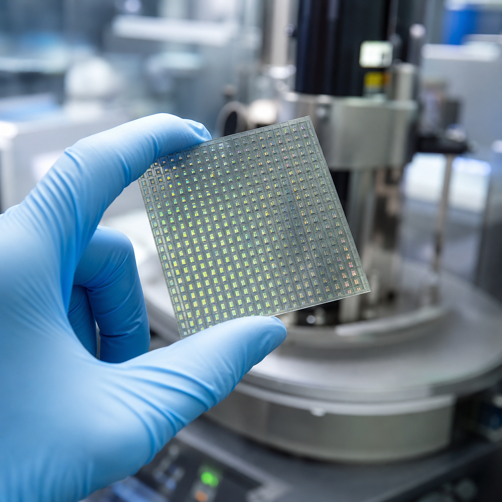
Innovations in polymers for advanced data storage solutions are reshaping how the electronics industry increases capacity, lowers energy use, and builds devices that remain reliable under severe thermal and mechanical stress. In this field, polymers are no longer limited to passive housings or cable coatings; they now function as dielectric layers, photoresists, flexible substrates, binders, encapsulants, separators, and nanoscale patterning media that directly affect how data is written, retained, moved, and protected. When engineers discuss advanced data storage, they usually mean technologies such as NAND flash, DRAM, emerging resistive memory, optical storage, magnetic tape, hard disks, and flexible or printed memory systems. Across all of these platforms, polymer science matters because storage density depends on precise structure at very small scales, and polymers are exceptionally tunable materials.
I have worked with electronics materials teams selecting polyimides, fluoropolymers, epoxy systems, and block copolymers for process integration, and the lesson is consistent: the right polymer can solve multiple bottlenecks at once. A dielectric with lower moisture uptake can improve signal stability and package reliability. A resist with sharper line-edge control can enable denser bit patterns. A substrate that survives repeated bending can turn a lab prototype of wearable memory into a manufacturable product. That is why polymers in high-tech and electronics deserve a hub article. They sit at the intersection of chemistry, device physics, semiconductor manufacturing, packaging, and lifecycle durability. Understanding recent innovations helps product teams choose materials that align with performance targets, manufacturing constraints, and long-term reliability expectations.
This overview explains how polymer innovation supports advanced data storage solutions, where each material class fits, what tradeoffs engineers must manage, and which application areas are driving the next wave of development. It also serves as a central map for deeper case studies within polymers in high-tech and electronics, connecting storage media, semiconductor memory, flexible devices, and protective packaging into one practical framework.
Why Polymers Matter in Modern Data Storage
Polymers matter in data storage because they offer a rare combination of processability, electrical tunability, low weight, mechanical compliance, and cost-effective large-area manufacturing. Silicon, metals, ceramic oxides, and magnetic alloys still perform the core information storage functions in most commercial devices, but polymer layers often determine whether those active materials can be patterned accurately and protected over years of use. In semiconductor memory fabrication, polymer photoresists are essential for lithography. In packaging, epoxy molding compounds and underfills protect chips from moisture, vibration, and thermal cycling. In flexible electronics, polymer substrates such as polyimide and polyethylene naphthalate allow memory arrays to bend without fracture.
At high densities, every nanometer matters. A polymer with poor dimensional stability can blur features during etch transfer. A polymer dielectric with excessive leakage or dielectric loss can degrade performance. A binder that does not distribute particles uniformly can reduce the reliability of a storage coating. The opposite is also true: well-designed polymers improve pattern fidelity, suppress parasitic effects, and stabilize interfaces. This is especially important as data storage devices face higher temperatures, thinner layers, and more aggressive scaling. Industry standards from JEDEC for memory reliability and IPC guidance for electronics assemblies reinforce the need for materials that maintain electrical and mechanical integrity across qualification testing.
Another reason polymers are central is manufacturing flexibility. Many polymer systems are compatible with spin coating, slot-die coating, inkjet printing, nanoimprint lithography, and roll-to-roll processes. These routes make polymers attractive for emerging nonvolatile memory, smart labels, edge devices, and flexible sensors with local storage. As electronics diversify beyond rigid boards and traditional chip packages, polymer-enabled integration becomes more valuable, not less.
Key Polymer Classes Used in High-Tech and Electronics
Several polymer families dominate advanced data storage solutions because each addresses a specific set of processing and performance requirements. Polyimides are widely used as flexible substrates and interlayer dielectrics due to their thermal stability, chemical resistance, and mechanical endurance. Epoxy systems appear in encapsulation, underfill, and adhesive applications because they cure into strong, dimensionally stable networks. Fluoropolymers provide low dielectric constants, chemical inertness, and moisture resistance, making them useful where signal integrity and environmental durability matter. Acrylics and methacrylates remain important in resist formulations and optical media coatings because they can be engineered for controlled exposure and development behavior.
Block copolymers represent one of the most significant innovations for high-density storage patterning. By designing chemically distinct polymer blocks that self-assemble into cylinders, lamellae, or other nanoscale domains, engineers can generate periodic patterns below the limits of conventional optical lithography. Polystyrene-block-poly(methyl methacrylate), often abbreviated PS-b-PMMA, became an early benchmark system because its domain formation is well studied and process conditions are well understood. More advanced high-chi block copolymers now deliver smaller feature sizes, which is essential for bit-patterned media and next-generation semiconductor pattern transfer.
Conductive and semiconductive polymers also deserve attention. Materials such as PEDOT:PSS, polyaniline derivatives, and donor-acceptor conjugated polymers are being investigated for printable memory devices and neuromorphic architectures. They are not replacing silicon flash in mainstream data centers, but they open new form factors for low-cost, low-temperature, and mechanically flexible storage. In practice, materials selection depends on glass transition temperature, coefficient of thermal expansion, dielectric constant, water absorption, outgassing behavior, adhesion to adjacent layers, and compatibility with etchants, solvents, and plasma steps.
| Polymer class | Primary storage-related role | Key advantage | Main limitation |
|---|---|---|---|
| Polyimides | Flexible substrates, insulating layers | High thermal stability and bend endurance | Moisture management and process complexity |
| Epoxies | Encapsulation, underfill, adhesives | Strong protection and dimensional stability | Brittleness if formulation is not optimized |
| Fluoropolymers | Low-k insulation, protective coatings | Low dielectric loss and chemical resistance | Adhesion can be difficult |
| Block copolymers | Nanoscale patterning media | Sub-lithographic feature formation | Defect control remains challenging |
| Conductive polymers | Printable memory and switching layers | Solution processing on flexible surfaces | Long-term stability varies by chemistry |
Polymer Innovations in Semiconductor Memory Fabrication
In semiconductor memory, polymer innovation often appears first in lithography and dielectric engineering. Photoresists are highly specialized polymer formulations containing resin systems, photoactive compounds, solvents, and additives tailored for ultraviolet or extreme ultraviolet exposure. As flash and DRAM feature sizes have shrunk, the industry has demanded better sensitivity, lower stochastic defect rates, stronger etch resistance, and tighter control over roughness. Chemically amplified resists have enabled many generations of scaling, but current process nodes require constant refinement because line collapse, acid diffusion, and photon shot noise become major limitations.
Directed self-assembly using block copolymers is one of the most practical answers to pattern density challenges. Instead of forcing all dimensions through increasingly expensive exposure tools, manufacturers can use guiding patterns from conventional lithography and let polymers self-organize into smaller periodic features. I have seen this approach evaluated not as a replacement for mainstream lithography, but as a complementary density multiplication technique. For storage applications, that matters in bit-patterned media research and in any memory architecture where regular arrays dominate the layout. Defectivity, placement control, and integration cost still need improvement, yet the materials science foundation is sound.
Low-k polymer dielectrics also support memory performance by reducing parasitic capacitance in interconnect structures. Lower capacitance means faster signal propagation and reduced cross-talk, both important in dense memory chips. However, low-k polymers can be mechanically weaker and more porous than traditional inorganic dielectrics, so integration requires careful balance. Plasma damage, metal diffusion, and moisture uptake can offset electrical gains if the stack is not engineered properly. The best results come from co-designing polymer chemistry with barrier layers, cure conditions, and package architecture rather than evaluating each material in isolation.
Flexible, Printed, and Wearable Memory Systems
One of the clearest growth areas for polymers in high-tech and electronics is flexible data storage. Traditional memory devices are fabricated on rigid silicon wafers, but emerging applications in medical patches, smart packaging, foldable displays, industrial sensors, and electronic textiles need storage on bendable surfaces. Polymer substrates make that possible. Polyimide remains the standard for high-temperature flexible circuits because it withstands soldering and many deposition processes. Polyethylene terephthalate and polyethylene naphthalate offer lower cost and optical transparency for less demanding thermal budgets.
Printed memory relies heavily on polymer processability. Solution-deposited dielectric layers, polymer ferroelectrics, and conductive polymer electrodes can be patterned at low temperatures on large areas. Poly(vinylidene fluoride) and its copolymers are notable because of their ferroelectric behavior, which enables nonvolatile memory effects in some device designs. Organic transistor memory and resistive switching elements using polymer matrices have shown promise for disposable electronics and edge devices that store small amounts of data locally. These systems will not challenge enterprise solid-state drives on capacity or endurance, but that is not the point. Their value lies in mechanical flexibility, low-cost fabrication, and compatibility with unconventional surfaces.
Real-world use depends on more than electrical switching. Flexible memory must survive repeated bending, humidity exposure, skin contact in wearables, and adhesive lamination. In test programs, the weak link is often the interface between a polymer substrate and a brittle conductive or oxide layer, not the substrate itself. Designers improve durability with neutral-plane engineering, stretchable interconnect geometries, and encapsulation stacks that limit oxygen and water ingress. As Internet of Things hardware spreads into logistics, healthcare, and consumer products, polymer-enabled flexible memory becomes a practical enabler rather than a niche research topic.
Polymers in Magnetic, Optical, and Archival Storage Media
Advanced data storage solutions are not limited to semiconductor memory. Polymers play a major role in magnetic and optical media, especially where coating uniformity, mechanical durability, and long-term stability determine usable life. Magnetic tape is a strong example. Modern enterprise tape cartridges still matter for cold storage because they offer low cost per terabyte and favorable energy economics for archives. The tape itself depends on polymer film substrates, typically polyethylene terephthalate or related materials, coated with magnetic particle layers dispersed in polymer binders. Improvements in binder chemistry, nanoparticle dispersion, and surface smoothness have increased areal density while reducing wear and dropouts.
Hard disk drives also use polymer materials in lubricants, protective overcoats, adhesives, cable assemblies, and suspension components, even though the magnetic recording layer is metallic. In these systems, tiny materials failures can cause catastrophic data loss, so contamination control, outgassing performance, and thermal aging behavior are tightly managed. Optical storage media similarly rely on polymers for substrates and protective coatings. Polycarbonate became standard in compact discs and DVDs because of its optical clarity and moldability. Advanced multilayer optical formats depend on polymer precision to maintain track geometry and laser readability.
For archival storage, stability over decades matters more than peak speed. Polymer oxidation, hydrolysis, ultraviolet degradation, and plasticizer migration are real risks. That is why archival media developers emphasize barrier coatings, antioxidant packages, and carefully controlled storage environments. ISO and IEC standards guide parts of media testing, but internal qualification often goes further, using accelerated aging to estimate retention under realistic conditions. When organizations evaluate long-term storage options, polymer durability should be treated as a core design variable, not a secondary packaging detail.
Packaging, Reliability, and Thermal Management
A storage device fails in the field more often because of packaging and interconnect problems than because a polymer looked good on a datasheet and bad in actual service. Encapsulation materials, underfills, lid sealants, adhesives, and thermal interface compounds all influence data retention and device lifespan. In solid-state drives and memory modules, epoxy molding compounds protect silicon dies from mechanical shock and humidity, while underfills distribute stress around solder joints in flip-chip assemblies. Without these polymer systems, thermal cycling would crack interconnects far more quickly.
Thermal management is especially important because data retention degrades as temperature rises. NAND flash charge leakage accelerates with heat, and package warpage can increase contact resistance or strain delicate structures. Polymers help by filling air gaps, bonding heat spreaders, and controlling coefficient of thermal expansion mismatch between silicon, substrates, and metal frames. The challenge is that many thermally conductive polymer formulations require ceramic fillers such as boron nitride or alumina, which can increase viscosity and complicate dispensing. Material selection therefore becomes a process integration exercise, not just a thermal calculation.
Reliability qualification typically includes highly accelerated stress testing, unbiased and biased humidity exposure, thermal shock, pressure cooker testing, and mechanical drop or vibration tests. Polymer innovations that reduce ionic contamination, lower moisture uptake, and improve adhesion directly improve pass rates. Engineers should also watch for subtle issues such as cure shrinkage, modulus drift after aging, and interactions with flux residues or cleaning chemistries. The best storage packages are built on conservative materials data, cross-sectional failure analysis, and close collaboration between polymer chemists and reliability engineers.
What Comes Next for Polymers in Advanced Data Storage Solutions
The next phase of innovation will center on finer patterning, lower-temperature manufacturing, better interface control, and more sustainable chemistries. In memory fabrication, expect continued work on high-chi block copolymers, molecular resists, and hybrid organic-inorganic materials that combine polymer processability with harder etch performance. In flexible electronics, the major push will be barrier films, printable dielectrics, and conductive polymers that retain function after repeated mechanical strain. For archival media, developers will continue improving binder stability, nanoparticle dispersion, and environmental resistance so that long-duration storage remains economical and dependable.
Sustainability is becoming a real design criterion. Solvent selection, fluorinated chemistry restrictions, cure energy, and recyclability now enter purchasing discussions earlier than they did a decade ago. Some bio-based monomers and solvent-free formulations are gaining attention, but they must still meet the uncompromising electrical and reliability standards of electronics manufacturing. No serious engineering team adopts a greener polymer if it introduces contamination, outgassing, or retention failures. Performance remains the gatekeeper.
For anyone evaluating polymers in high-tech and electronics, the practical takeaway is simple: treat polymers as functional materials that shape storage performance, manufacturability, and lifetime, not as commodity support layers. The strongest programs define application requirements first, map them to polymer properties, validate those properties under realistic stress conditions, and then refine the full stack as a system. Use this hub as your starting point for deeper case studies on flexible electronics, semiconductor packaging, magnetic media, and printable memory. The right polymer decision can unlock higher density, better reliability, and more adaptable data storage products.
Frequently Asked Questions
1. How are polymers being used directly inside advanced data storage devices rather than just as protective materials?
Modern data storage design relies on polymers for far more than insulation, housings, or cable jackets. In advanced devices, specialized polymers act as functional materials that influence how information is written, read, stored, and protected over time. They are used as dielectric layers in memory structures, where their electrical properties help control charge behavior and reduce unwanted leakage. In lithography and nanoscale manufacturing, polymer-based photoresists and patterning materials enable the precise formation of extremely small features that are essential for increasing storage density. Flexible polymer substrates also support thin, lightweight, and bendable storage formats, opening possibilities for wearable electronics, foldable systems, and embedded sensing platforms.
Polymers also serve as binders, encapsulants, separators, and interfacial layers in storage-related architectures. In these roles, they help maintain mechanical integrity, isolate sensitive components, and protect against moisture, oxidation, contamination, and thermal cycling. In emerging memory technologies, polymer chemistry can be tuned to improve surface smoothness, adhesion, dielectric constant, ion transport, and compatibility with metals, semiconductors, and nanomaterials. That tunability is one of their greatest advantages. Unlike many traditional inorganic materials, polymers can be engineered at the molecular level to balance electrical performance, processability, flexibility, and durability. As a result, they are becoming central to the performance of solid-state drives, non-volatile memory, flexible data systems, and next-generation storage platforms that must operate reliably in demanding environments.
2. Why are polymer innovations important for increasing storage capacity and reducing energy consumption?
Storage capacity and energy efficiency depend heavily on how precisely a device can manage charge, isolate signals, and support miniaturized architectures. Advanced polymers contribute to all three. As data storage features shrink to nanoscale dimensions, materials must maintain electrical control without introducing defects, leakage currents, or instability. High-performance polymer dielectrics and polymer-derived nanoscale patterning media help manufacturers create smaller and more densely packed structures, which directly supports higher bit density and greater overall capacity. Because polymers can often be processed into ultra-thin, uniform films, they are especially useful where dimensional control and smooth interfaces are critical.
On the energy side, polymer materials can lower power requirements by improving insulation, reducing parasitic losses, and enabling lower-voltage operation in certain memory architectures. Their dielectric properties can be tailored to support efficient switching behavior, while their low-weight and solution-processable nature can reduce manufacturing energy compared with some conventional materials and fabrication routes. In flexible and portable electronics, lightweight polymer components also help reduce total system demands. Equally important, polymers can improve thermal management indirectly by preserving structural stability and insulating sensitive regions, which helps devices operate more efficiently under real-world conditions. In short, polymer innovation supports denser memory, cleaner signal behavior, lower power draw, and more scalable manufacturing, all of which are key to modern data storage advancement.
3. What makes polymers suitable for data storage devices that must withstand severe thermal and mechanical stress?
Data storage systems increasingly operate in harsh conditions, including elevated temperatures, repeated thermal cycling, vibration, bending, compression, and long service life expectations. Polymers are well suited to these challenges because they can be formulated to combine thermal stability, mechanical toughness, chemical resistance, and strong adhesion across complex multilayer structures. High-performance polymer families can retain their structural and electrical properties under substantial heat loads, making them useful for encapsulation, dielectric isolation, flexible circuitry, and interface protection. This is especially important in automotive electronics, industrial control systems, aerospace hardware, edge computing devices, and high-density memory packages, where failure can result from cracking, delamination, moisture ingress, or dielectric breakdown.
Another major advantage is that polymers can absorb or redistribute stress more effectively than many brittle materials. In multilayer assemblies with different coefficients of thermal expansion, engineered polymer layers help reduce stress concentrations and protect delicate features from fracture or fatigue. Flexible substrates and compliant interlayers are particularly valuable in bendable and miniaturized storage devices, where rigidity can become a reliability problem. At the same time, advanced barrier polymers and encapsulants shield sensitive memory elements from oxygen, solvents, and humidity that can degrade performance over time. When researchers talk about reliability in advanced storage, they are increasingly talking about polymer design, because these materials influence not only whether a device survives environmental stress, but also whether it continues to retain data accurately after prolonged use.
4. Which polymer properties matter most in next-generation memory and storage applications?
The most important polymer properties depend on the storage technology, but several characteristics consistently matter across applications. Electrical behavior is at the top of the list. Dielectric constant, breakdown strength, leakage control, charge trapping behavior, and interfacial stability all affect how efficiently a storage device can operate and how well it retains information. For nanoscale fabrication, film uniformity, line-edge definition, and pattern fidelity are equally critical, especially in polymer photoresists and self-assembling materials used to create dense memory arrays. In flexible electronics, mechanical properties such as modulus, elongation, fatigue resistance, and dimensional stability become central because the material must survive repeated bending or deformation without compromising electrical function.
Thermal properties are also essential. Glass transition temperature, decomposition resistance, thermal conductivity, and coefficient of thermal expansion influence both manufacturing compatibility and long-term reliability. In storage systems assembled with metals, ceramics, and semiconductor layers, polymers must bond well and remain stable across multiple processing steps. Chemical resistance, moisture barrier performance, and low outgassing are especially important in tightly packed electronics where contamination can damage device behavior. Processability matters too: polymers that can be deposited as thin films, patterned accurately, cured at manageable temperatures, or integrated into roll-to-roll and additive manufacturing workflows offer significant commercial advantages. The most successful polymer systems are rarely chosen for just one property; they are selected because they deliver a balanced package of electrical, thermal, mechanical, chemical, and manufacturing performance.
5. What future developments in polymer science could have the biggest impact on advanced data storage solutions?
Some of the most promising developments involve polymers designed with highly specific molecular architectures to perform targeted roles in memory systems. One major area is the creation of next-generation dielectric and ferroelectric polymers that support faster switching, improved charge retention, and lower operating voltages. Another is block copolymer and self-assembly research, which could enable extremely fine nanoscale patterning beyond the practical limits of conventional lithography alone. These materials may help manufacturers build denser storage arrays with better consistency and lower cost. Conductive and semiconductive polymers are also attracting interest for use in emerging memory concepts, neuromorphic hardware, and hybrid organic-inorganic storage platforms.
Beyond electrical function, future progress will likely come from multifunctional polymers that combine several benefits in a single material system. For example, researchers are pursuing polymers that offer strong dielectric performance while also acting as moisture barriers, thermal stabilizers, or self-healing protective layers. Sustainable polymer chemistry is another important direction, especially as electronics manufacturers seek lower-impact materials, safer solvents, and more recyclable device components. Advances in nanocomposite polymers, where polymer matrices are combined with graphene, ceramic nanoparticles, or other nanoscale additives, could further improve thermal transport, mechanical strength, and electrical precision. Over time, the biggest impact may come from polymers that are not simply substituted into existing device designs, but that enable entirely new storage architectures, manufacturing methods, and form factors that would be difficult or impossible with traditional materials alone.