Flexible electronics moved from laboratory demonstrations to commercial reality because polymers solved problems that silicon, glass, and brittle metal oxides could not. In this case study on polymers in flexible electronics, the focus is successful polymer applications: which materials worked, where they were deployed, why they succeeded, and what engineers learned while scaling them. Flexible electronics refers to electronic devices built on bendable, stretchable, or conformable substrates that continue functioning under mechanical deformation. Polymers are long-chain organic materials used here as substrates, dielectrics, semiconductors, encapsulants, adhesives, conductors, and barrier layers. I have worked on device qualification programs where the polymer stack, not the transistor architecture, determined whether a product passed humidity aging and bending fatigue. That experience mirrors the wider industry: performance depends on the whole materials system.
The category matters because demand now spans foldable displays, wearable biosensors, e-textiles, smart labels, medical patches, soft robotics, and lightweight solar modules. Each application asks the same practical questions. Can the device survive repeated bending at a small radius? Can it be manufactured by roll-to-roll coating, printing, or lamination at temperatures below the limit of plastic substrates? Can it resist oxygen, water vapor, sweat, skin oils, and cleaning chemicals? Can it do so at a cost that fits consumer, industrial, or healthcare margins? Polymers make these answers possible because they combine low density, tunable chemistry, and process compatibility with large-area manufacturing. They also introduce tradeoffs, especially in gas permeability, dimensional stability, and long-term creep, which is why understanding successful polymer applications requires case-by-case analysis rather than broad claims.
This hub article surveys the most important classes of polymer success in flexible electronics and connects them into a practical framework. It covers high-performance substrate polymers such as polyimide and polyethylene terephthalate, conductive and semiconducting polymers including PEDOT:PSS and polythiophenes, polymer dielectrics and encapsulation systems, and composite approaches that blend polymers with silver nanowires, carbon nanotubes, graphene, or metal flakes. It also examines how products passed from prototyping to manufacturing through reliability testing, interface engineering, and process control. Readers looking across the successful polymer applications landscape will find a clear pattern: the winning designs matched polymer chemistry to mechanical strain, moisture exposure, and manufacturing temperature from the beginning, not as an afterthought.
Why polymers became the enabling platform
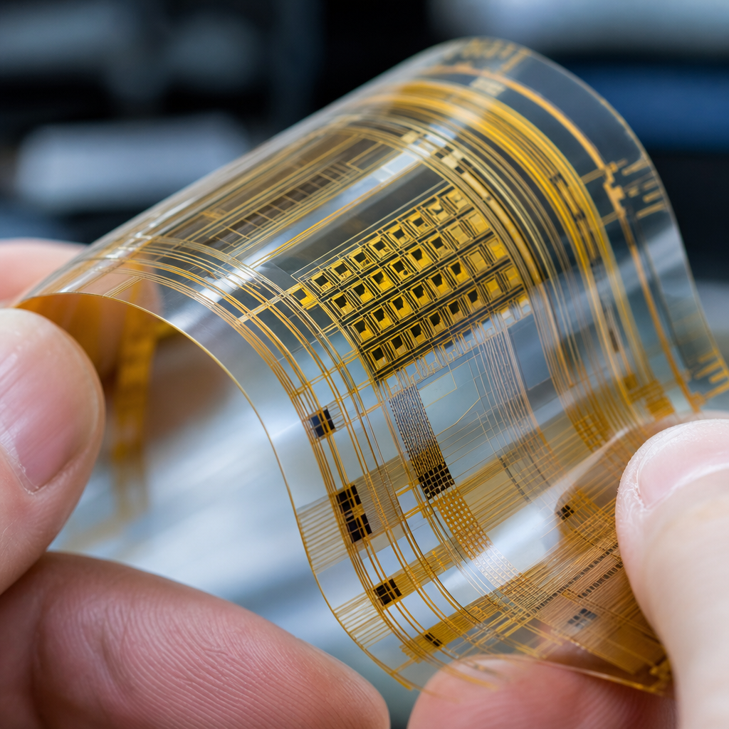
Polymers became central to flexible electronics because they decouple function from rigidity. Traditional microelectronics relied on crystalline silicon wafers and glass panels that delivered excellent dimensional control but resisted bending. By contrast, polymer films can be cast, stretched, coated, laser patterned, embossed, and laminated into multilayer stacks that absorb strain. Polyimide became the benchmark substrate for high-temperature processing because it retains mechanical integrity well above 300°C and offers good dielectric performance. PET and polyethylene naphthalate gained broad use where cost, transparency, and high-throughput web handling mattered more than extreme heat resistance. Thermoplastic polyurethane and silicone elastomers opened stretchable formats for epidermal sensors by tolerating elongation that rigid films cannot survive.
In practice, the choice was rarely about a single material property. Successful products balanced modulus, coefficient of thermal expansion, surface energy, optical haze, moisture uptake, and line compatibility. A foldable display stack, for example, needs low birefringence, optical clarity, scratch resistance, and a neutral plane design that keeps brittle layers near the region of lowest strain. A disposable biosensor patch needs skin comfort, biocompatible adhesives, and electrical stability after exposure to sweat. In projects I have seen succeed, teams stopped treating the polymer as packaging and treated it as part of the active device architecture. That shift improved adhesion, reduced cracking at interfaces, and shortened rework cycles during pilot production.
Case study: display backplanes and foldable devices
The strongest high-visibility proof of successful polymer applications is the foldable display market. Flexible OLED panels rely heavily on colorless polyimide or advanced transparent polymer cover layers because standard glass cannot tolerate repeated folding without fracture. In these systems, polymers appear at multiple levels: the substrate supports thin-film transistors, planarization layers smooth surface roughness, polyimide serves as an insulating and stress-buffering film, pressure-sensitive adhesives bond optical stacks, and encapsulation polymers protect oxygen-sensitive organic emitters. The engineering target is demanding. OLED materials degrade rapidly when exposed to moisture and oxygen, and the fold radius may be only a few millimeters. The polymer stack therefore needs both flexibility and barrier performance, often achieved through hybrid thin-film encapsulation that alternates inorganic layers such as Al2O3 or SiNx with polymer decoupling interlayers.
Commercial success depended on solving crack initiation and delamination rather than simply proving bendability once. Repeated folding induces cyclic strain, and if the neutral plane is misplaced, brittle conductive oxides and barrier layers fail early. Manufacturers used finite element modeling, dynamic mechanical analysis, and accelerated fold tests to optimize stack symmetry and adhesive modulus. A lower-modulus optically clear adhesive can redistribute stress, but if it creeps excessively at elevated temperature, display mura and alignment drift appear. The winning solutions paired high-performance polyimide substrates with carefully selected acrylic or silicone-based adhesives and multilayer barriers. This is why flexible display reliability is a polymer engineering story as much as an electronics story.
Case study: conductive polymers in touch, sensing, and biointerfaces
Conductive polymers provided another route to success by replacing brittle transparent electrodes or enabling intimate contact with soft surfaces. PEDOT:PSS is the best-known example. It is a water-dispersible conductive polymer system used in antistatic coatings, hole transport layers, organic photovoltaics, neural interfaces, and wearable sensors. Its practical appeal is straightforward: it can be coated or printed at low temperature, forms smooth films, and remains functional under bending where indium tin oxide often cracks. Conductivity can be raised dramatically through formulation and post-treatment using solvents such as dimethyl sulfoxide or ethylene glycol, though those gains must be balanced against environmental stability and film uniformity. In several wearable sensor programs, PEDOT:PSS succeeded because it produced lower interfacial impedance against skin or tissue than stiffer metallic electrodes.
Bioelectronic case studies show why polymers win where conventional materials plateau. Soft electrode arrays for electrophysiology need conformability to reduce motion artifacts and maintain contact on curved, moving tissue. Conductive polymer coatings on gold or platinum electrodes lower impedance and improve charge transfer, which directly benefits signal quality in ECG, EMG, and neural recording systems. The same logic applies to skin patches that monitor hydration, temperature, or strain. Polymer electrodes and interconnects embedded in elastomers stretch with the body, making long-wear measurements more reliable than rigid islands alone. The limitation is not whether conductive polymers work; it is whether the formulation remains stable under sweat, sterilization, UV exposure, and repeated strain. Successful applications solved that by adding crosslinkers, encapsulating edges, and validating drift through long-duration wear studies.
Case study: polymer semiconductors in printed circuits and RFID
Organic semiconducting polymers transformed printed electronics by enabling transistor fabrication on plastic films at low temperature over large areas. Materials based on polythiophene derivatives, diketopyrrolopyrrole copolymers, and related donor-acceptor backbones have been used in thin-film transistors for sensors, smart packaging, and low-cost logic. Their greatest commercial value appears where ultra-high speed is unnecessary but mechanical flexibility, thinness, and area coverage are critical. Radio-frequency identification tags, shelf labels, and disposable diagnostic strips benefit from this profile. Printing or coating these semiconductors by slot-die, gravure, or inkjet can reduce material waste relative to vacuum deposition, and the process fits roll-to-roll manufacturing better than conventional wafer methods.
The success factors were surprisingly mundane. Device mobility mattered, but yield mattered more. Printed polymer transistor circuits only became commercially relevant when manufacturers improved solvent orthogonality, registration control, and dielectric interface quality. A semiconducting polymer can show impressive mobility in a paper, yet fail in production because contact resistance drifts or morphology varies across a web. Successful programs used surface treatment, annealing windows, and statistical process control to lock down film formation. They also targeted realistic use cases: simple sensor readout, memory elements, and flexible logic rather than trying to replace high-end silicon computing. That disciplined application matching is a recurring theme across successful polymer applications.
Case study: substrates, dielectrics, and encapsulation layers
Many of the most commercially successful polymer applications are invisible to end users because they sit beneath the active circuitry. Substrate films such as PET, PEN, and polyimide define the thermal budget and web handling behavior of an entire line. Dielectric polymers such as poly(methyl methacrylate), crosslinked acrylics, fluoropolymers, parylene, and photo-patternable polyimides determine leakage current, capacitance stability, and interlayer reliability. Encapsulation materials then decide shelf life. In barrier-sensitive products, a polymer alone is rarely enough because water vapor transmission rates are too high. The strongest solutions use multilayer architectures: polymer for flexibility and crack arrest, inorganic nanolayers for barrier performance, and edge seals to block ingress at cut surfaces. This approach is standard in OLED, flexible photovoltaics, and moisture-sensitive sensors.
| Polymer role | Common materials | Why it succeeds | Main limitation |
|---|---|---|---|
| Substrate | Polyimide, PET, PEN | Lightweight, bendable, compatible with web processing | Thermal expansion and moisture sensitivity vary by grade |
| Conductor or electrode aid | PEDOT:PSS, silver-polymer composites | Low-temperature coating, good bending endurance | Conductivity and environmental stability need optimization |
| Semiconductor | Polythiophenes, DPP copolymers | Printable over large areas on plastic | Lower speed and tighter process window than silicon |
| Dielectric and encapsulant | Acrylics, fluoropolymers, parylene, epoxies | Electrical insulation, planarization, stress buffering | Barrier performance often needs hybrid multilayers |
In qualification work, encapsulation failures often appeared first at corners, vias, and flexed edge regions. That is why successful teams measured not just bulk water vapor transmission rate but also adhesion after damp heat, crack propagation after cyclic bending, and outgassing effects on nearby layers. Test methods commonly combined mandrel bend testing, IPC-style environmental exposures, peel strength measurement, optical inspection, and electrical drift tracking. Materials that looked equivalent in datasheets separated quickly under these conditions. The practical lesson is simple: a polymer system succeeds when it survives interfaces and defects, not only when it performs in ideal flat-film measurements.
Case study: energy, healthcare, and emerging wearable systems
Flexible solar cells, batteries, and medical wearables demonstrate how polymers enable entirely new product formats. In organic photovoltaics and perovskite-flex concepts, polymer substrates and barrier films allow lightweight modules that conform to curved surfaces, useful for portable charging and building-integrated applications. In printed batteries and supercapacitors, polymer binders and separators govern ionic transport, coating quality, and mechanical durability. Healthcare offers perhaps the clearest evidence of value. Continuous glucose monitors, ECG patches, smart wound dressings, and rehabilitation sleeves all depend on polymer adhesives, encapsulants, and flexible circuit carriers. These components must tolerate movement while remaining comfortable for hours or days, and they must maintain signal quality despite sweat and changing skin topography.
Successful medical and wearable applications share three traits. First, they prioritize biocompatibility and irritation control alongside electrical performance. Second, they design for realistic strain paths, placing rigid chips on islands and routing polymer-supported interconnects through serpentine traces. Third, they validate under use conditions, not only bench conditions. A patch that works on dry skin in a lab may fail after showering, exercise, or overnight wear. Teams that succeed combine polymer selection with human factors testing, package sealing, and adhesive tuning. Looking ahead, recyclable substrates, bioresorbable polymers, self-healing elastomers, and lower-temperature conductive inks will expand what flexible electronics can do. The core lesson remains unchanged: polymers succeed when chosen as functional engineering materials with quantified tradeoffs, not as generic plastics.
Polymers in flexible electronics have succeeded because they solved the exact constraints that blocked adoption: brittleness, weight, processing temperature, and poor conformity to moving surfaces. The strongest case studies span foldable displays, wearable sensors, printed circuits, RFID, biointerfaces, and lightweight energy devices. Across all of them, success came from using polymers in multiple roles at once: substrate, dielectric, semiconductor, conductor support, adhesive, and encapsulant. Materials such as polyimide, PET, PEN, PEDOT:PSS, parylene, acrylics, and semiconducting polythiophenes delivered value not in isolation but as coordinated stacks engineered for strain, humidity, and manufacturing flow. That is the central pattern linking successful polymer applications across the entire subtopic.
For readers using this page as a hub under case studies and applications, the practical takeaway is to evaluate any polymer-enabled device through four questions. What deformation must it survive? What environment will it face? What process temperature and throughput are required? Which interfaces are most likely to fail first? Answer those questions early and the right polymer family usually becomes clear. Ignore them and even promising electrical designs stall in qualification. If you are building your own roadmap around successful polymer applications, use this article as the starting framework, then map each downstream topic—displays, healthcare, printed sensors, energy, and packaging—against the same reliability-driven material logic.
Frequently Asked Questions
Why are polymers so important in flexible electronics compared with traditional materials like silicon, glass, and metal oxides?
Polymers became foundational to flexible electronics because they address the exact limitations that made conventional electronic materials difficult to use in bendable devices. Traditional silicon wafers, glass substrates, and many metal oxides perform extremely well in rigid electronics, but they are inherently brittle, heavy, or prone to cracking under repeated bending. Polymers, by contrast, can be engineered to be lightweight, mechanically compliant, chemically tunable, and compatible with large-area processing. That combination made them uniquely suited for devices that need to flex, roll, stretch, or conform to curved surfaces.
In real commercial deployments, polymers succeeded not just because they were flexible, but because they served multiple functions at once. A single polymer class could act as a substrate, dielectric, encapsulant, conductive layer, adhesive, or barrier coating. Materials such as polyimide enabled flexible printed circuits and display backplanes because they could tolerate relatively high processing temperatures while maintaining dimensional stability. Conductive polymers like PEDOT:PSS proved valuable in electrodes and hole-transport layers because they offered transparency, solution processability, and better mechanical resilience than brittle transparent conductive oxides alone. Elastomeric polymers opened the door for stretchable sensors and skin-like interfaces by allowing electronics to move with the body rather than resist it.
What engineers learned is that the value of polymers lies in system-level performance, not just material substitution. Flexible electronics only became commercially viable when polymer materials were matched carefully to device architecture, manufacturing method, and use environment. The winning polymer solutions were the ones that combined bendability with manufacturability, reliability, and cost control. In that sense, polymers did not merely replace rigid materials; they changed how flexible devices were designed, fabricated, and scaled.
Which polymer materials have been most successful in flexible electronics, and where have they actually been used?
Several polymer families stand out as real success stories because they moved beyond laboratory prototypes into meaningful commercial and near-commercial applications. Polyimide is one of the clearest examples. It has been widely used as a flexible substrate in foldable displays, flexible printed circuit boards, wearable components, and sensor assemblies because it offers excellent thermal resistance, strong mechanical durability, and good chemical stability. Engineers favored it when manufacturing workflows required elevated temperatures or tight dimensional control. In many flexible display stacks, colorless polyimide also became important as a substitute for glass-like cover layers where impact resistance and bendability were critical.
Polyethylene terephthalate, or PET, and polyethylene naphthalate, or PEN, also achieved broad use, especially in lower-temperature, roll-to-roll compatible electronics. These materials found applications in flexible touch sensors, printed RFID tags, smart labels, disposable medical sensors, and low-cost display components. Their main advantage was economic scalability: they could be processed over large areas using printing and coating technologies, making them practical for high-volume manufacturing where extreme thermal performance was not required.
Among functional polymers, PEDOT:PSS is one of the most cited examples of a successful conductive polymer. It has been deployed in organic electronics, transparent electrodes, antistatic coatings, wearable sensors, and bioelectronic interfaces. Its appeal came from a rare combination of conductivity, optical transparency, and compatibility with solution-based deposition. Meanwhile, fluoropolymers, acrylics, silicones, epoxies, and polyurethane-based systems have been used extensively as encapsulation layers, dielectrics, adhesives, and stretchable matrices in medical patches, e-textiles, flexible batteries, and soft sensor platforms.
The practical lesson from these deployments is that no single polymer “won” flexible electronics. Instead, the field advanced through specialized materials succeeding in specific roles. Polyimide dominated where heat resistance and mechanical endurance mattered. PET and PEN succeeded where cost and throughput were decisive. Conductive and semiconducting polymers gained ground where solution processing and mechanical compliance offered a clear advantage. The most successful products were almost always multilayer systems in which each polymer was selected for a defined engineering function.
What made certain polymer applications succeed commercially while others remained stuck in the prototype stage?
The polymer applications that succeeded commercially did so because they solved a complete product problem rather than demonstrating an impressive material property in isolation. In the lab, a polymer may show excellent flexibility, conductivity, or stretchability, but commercialization depends on a broader set of requirements: stable electrical performance over time, compatibility with manufacturing equipment, resistance to moisture and oxygen, acceptable cost, and reliable behavior under real-world use. Many early flexible electronics concepts failed to scale because they optimized one headline metric while overlooking process yield, interlayer adhesion, shelf life, or environmental durability.
Successful applications usually shared four traits. First, they fit an application where flexibility created real value rather than novelty. Wearable health patches, foldable displays, flexible circuits, and conformable sensors all benefited from polymers because the end product genuinely needed to bend or conform. Second, the selected polymers matched the manufacturing route. Materials that worked with printing, coating, lamination, or low-temperature deposition often scaled more smoothly than those requiring narrowly controlled laboratory steps. Third, the polymer layers had to integrate into a full stack without causing new failure modes such as cracking at interfaces, solvent damage, creep under stress, or permeability-related degradation. Fourth, manufacturers needed supply chain consistency. A polymer that performs beautifully in a research batch but varies from lot to lot is rarely suitable for volume electronics.
Engineers also learned that commercial success often came from pragmatic compromise. A polymer did not need to be the most conductive, the most transparent, or the most stretchable in the literature. It needed to be good enough across all critical metrics at production scale. That is why some seemingly modest materials became industry standards while more advanced alternatives remained experimental. The winners were dependable, process-friendly, and economically realistic. In flexible electronics, commercial success was driven less by the most exotic polymer chemistry and more by balanced engineering performance.
What were the biggest engineering challenges when scaling polymer-based flexible electronics from the lab to manufacturing?
Scaling polymer-based flexible electronics exposed a very different set of challenges than proving a concept in the lab. One of the most important issues was dimensional and mechanical stability during processing. Polymers can expand, shrink, warp, absorb moisture, or relax under thermal and mechanical stress. In a laboratory sample, that may be manageable. In roll-to-roll production or multilayer device assembly, even small dimensional shifts can ruin alignment, reduce yield, or create electrical defects. Engineers had to understand not just the polymer’s nominal properties, but how it behaved under every thermal, solvent, coating, and curing step in the line.
Barrier performance was another major hurdle. Many flexible electronic components, especially organic semiconductors and sensitive electrodes, degrade when exposed to oxygen and moisture. Polymers are usually more permeable than glass or metal foils, so encapsulation became a critical area of innovation. The best-performing systems often relied on hybrid barrier stacks that combined polymer layers with inorganic thin films to reduce permeation while preserving flexibility. This was a key lesson in the field: polymers enabled flexibility, but they often needed help to match the environmental protection of rigid packaging technologies.
Interface reliability also proved difficult. A flexible device is usually a laminated stack of materials with very different mechanical moduli, thermal expansion coefficients, and surface chemistries. Under repeated bending, those mismatches can lead to delamination, microcracking, resistance drift, or catastrophic failure. Engineers had to develop better adhesion promoters, neutral-plane designs, strain-relief geometries, and layer thickness optimization to distribute stress more effectively. In many successful products, structural design mattered just as much as material selection.
Finally, manufacturing economics forced discipline. Lab processes that depended on slow deposition, exotic solvents, tightly controlled atmospheres, or difficult patterning methods often could not compete commercially. The transition to scalable production favored polymers that could be coated uniformly, patterned reproducibly, and handled at high throughput. The main takeaway for engineers was clear: in flexible electronics, scale-up is not an afterthought. Material choice, device architecture, and process design have to be developed together from the beginning if polymer-based concepts are to become manufacturable products.
What key lessons did engineers learn from successful case studies of polymers in flexible electronics?
The most important lesson was that flexible electronics is a systems engineering challenge, not simply a materials challenge. Early enthusiasm often focused on discovering a remarkable polymer with one standout property, such as very high conductivity or extreme stretchability. But successful case studies showed that device reliability depends on how polymers interact with every other layer, process step, and use condition. Engineers learned to evaluate polymers in context: as part of an integrated mechanical, electrical, thermal, and manufacturing system.
Another major lesson was that application-specific optimization beats universal solutions. A polymer ideal for a foldable display is not necessarily ideal for a disposable biosensor or a stretchable skin patch. For displays, optical clarity, thermal endurance, and low haze may be decisive. For wearables, softness, biocompatibility, breathability, and fatigue resistance may matter more. For printed tags and smart packaging, material cost and roll-to-roll process compatibility can outweigh premium performance. The strongest case studies succeeded because developers aligned polymer selection tightly with end-use requirements instead of chasing a one-size-fits-all platform.
Engineers also learned to respect failure over time.