Polymers have become one of the decisive materials behind the miniaturization of modern electronics, enabling thinner circuits, lighter packages, flexible devices, and manufacturing methods that silicon and metals alone cannot deliver. In electronics, miniaturization means reducing the size and weight of components while preserving or improving electrical performance, heat management, reliability, and production efficiency. Polymers are long-chain molecules engineered to provide insulation, mechanical protection, dielectric control, adhesion, optical clarity, chemical resistance, and increasingly, active electrical functions. In practice, I have seen polymer selection determine whether a design reaches smartwatch dimensions, survives solder reflow, or fails during humidity testing. That is why polymers matter across the full electronics stack, from chip packaging and printed circuit boards to sensors, displays, batteries, medical wearables, and automotive control units.
The importance of polymers in high-tech electronics is easiest to understand by looking at what miniaturization demands. Smaller devices require tighter line spacing, thinner insulating layers, lower dielectric loss, lower stress on solder joints, and materials that can be processed at scale. Traditional materials such as ceramics, glass, and metals still play critical roles, but they are often rigid, heavy, brittle, or expensive to fabricate into ultrathin forms. Advanced polymers close these gaps. Polyimides, liquid crystal polymers, epoxies, silicones, fluoropolymers, polyether ether ketone, and engineered acrylics each solve different constraints. Some support high-frequency signal integrity, others withstand temperatures above 250°C, and others permit roll-to-roll fabrication for flexible electronics. As devices move into 5G, electric vehicles, implantables, and edge sensors, polymer engineering increasingly shapes what can be made, how small it can be, and how reliably it performs over years of service.
Why polymers are essential in electronic miniaturization
Miniaturization is not simply shrinking a part; it is reducing volume without creating unacceptable electrical, thermal, or mechanical penalties. Polymers enable this by combining low density with tunable properties. A dielectric film can be made only micrometers thick, yet still isolate conductive traces. An underfill can protect fine-pitch solder bumps beneath a chip-scale package. A flexible substrate can bend around a wrist or fit within a catheter. These are not marginal conveniences. They are the difference between board-level assembly and system-in-package integration, between a rigid module and a foldable product.
One reason polymers are so effective is process compatibility. Semiconductor packaging, surface-mount assembly, photolithography, inkjet printing, laser drilling, and lamination all rely on materials that can flow, cure, pattern, or bond predictably. In production lines I have worked with, replacing a standard epoxy with a lower-modulus formulation reduced stress cracking in miniature sensors because the package could better absorb thermal mismatch between silicon, copper, and the surrounding housing. That same principle applies widely. A polymer does not need to conduct electricity to be high value in electronics; often, its real contribution is letting conductive materials be packed closer together without failure.
Polymers also help lower cost and increase throughput. Injection molding creates precise housings and connectors at high volumes. Thin polymer films can be coated continuously. Adhesives replace bulky fasteners. Encapsulants reduce moisture ingress and mechanical shock. For consumer electronics, this allows compact devices at mass-market price points. For aerospace or medical devices, it enables performance where every gram and cubic millimeter matter.
Core polymer families used in high-tech electronics
Different polymer classes serve distinct functions, and understanding their roles is essential when evaluating electronic design options. Polyimide is a leading material for flexible printed circuits because it maintains dimensional stability and dielectric performance under heat. Kapton, the well-known DuPont polyimide film, is widely used in flex circuits, insulating tapes, and space electronics. Liquid crystal polymer, or LCP, offers low moisture absorption and excellent high-frequency properties, making it valuable for antennas, connectors, and compact RF modules. Epoxy systems dominate in printed circuit board laminates, encapsulation, and semiconductor packaging because they bond well and can be formulated for strength, thermal resistance, and controlled flow.
Silicones are often selected where softness, thermal stability, and environmental sealing are needed. In LED assemblies and power modules, silicone materials can outperform more brittle alternatives because they tolerate repeated thermal cycling. Fluoropolymers such as PTFE and FEP provide extremely low dielectric constants and chemical resistance, supporting high-frequency communication hardware and harsh-environment electronics. PEEK appears in connectors, insulation, and precision components where high strength and sterilization resistance are required. Conductive polymers, though still more specialized than structural polymers, are important in antistatic coatings, organic electronics, printed sensors, and certain capacitor systems.
The right material depends on a balance of glass transition temperature, coefficient of thermal expansion, dielectric constant, dissipation factor, moisture uptake, modulus, adhesion, and chemical resistance. Engineers also assess outgassing, UL flammability ratings, reflow survivability, and compatibility with lead-free soldering profiles. A polymer that works well in a consumer earbud may fail in an under-hood automotive radar module because the temperature and humidity profile is entirely different.
Applications across packaging, circuit design, and flexible systems
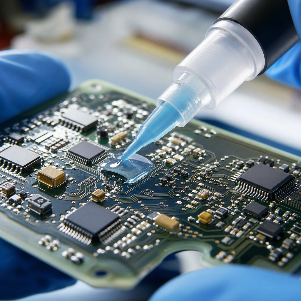
Semiconductor packaging is one of the clearest examples of how polymers support miniaturization. In ball grid array, flip-chip, and wafer-level packages, polymer materials appear as die attach films, underfills, mold compounds, passivation layers, and redistribution dielectrics. As bump pitch decreases, these materials must fill smaller gaps, cure with low voiding, and limit warpage. A poorly chosen underfill can create delamination after temperature cycling; a well-chosen one dramatically extends package life. Epoxy mold compounds with silica fillers remain central to protecting chips while keeping package size compact.
Printed circuit boards also rely heavily on polymers. Standard FR-4 uses woven glass and epoxy resin, but high-density interconnect boards require finer vias, thinner cores, and better dielectric control than legacy systems. Build-up films and solder masks are polymeric layers engineered for photopatterning and insulation. In smartphones, multilayer boards and rigid-flex assemblies use polymer films to route signals through extremely constrained spaces. Flexible printed circuits based on polyimide replace bulkier wiring harnesses and improve reliability in hinge areas, camera modules, and compact medical instruments.
Display technology offers another strong case. Organic light-emitting diode devices use multiple polymer-related layers, from substrates and encapsulants to alignment and barrier materials. Foldable and rollable displays would not exist in commercially viable form without polymer substrates that can flex repeatedly while maintaining optical and electrical integrity. In sensors, polymers appear in membranes, microfluidic channels, wearable patches, and dielectric layers for capacitive sensing. In batteries, separators and binders are polymer-based and directly affect safety, thickness, and cycle life.
| Application area | Common polymers | Miniaturization benefit | Typical example |
|---|---|---|---|
| Flexible circuits | Polyimide, acrylic adhesive, LCP | Thin routing in tight spaces | Smartphone camera module |
| Chip packaging | Epoxy mold compounds, underfills, silicones | Smaller, protected semiconductor packages | Flip-chip processor package |
| RF electronics | LCP, PTFE, fluoropolymers | Low signal loss at high frequency | 5G antenna module |
| Wearables and medical devices | Silicones, TPU, PEEK, polyimide | Lightweight, conformable assemblies | Continuous glucose monitor |
| Displays | Polyimide, barrier coatings, acrylics | Flexible and ultra-thin screens | Foldable OLED display |
Performance tradeoffs engineers must manage
Polymers solve many miniaturization problems, but they introduce tradeoffs that must be managed carefully. Thermal conductivity is a common limitation. Most polymers are natural insulators, which is useful electrically but problematic when compact devices generate significant heat. Fillers such as boron nitride, alumina, or aluminum nitride can improve thermal performance, though they may increase viscosity, cost, or brittleness. In dense packages, engineers often combine polymer dielectrics with metallic heat spreaders, graphite sheets, or vapor chambers.
Moisture absorption is another critical issue. Some polymers swell or shift dielectric properties when exposed to humidity, which can degrade RF performance or create reliability problems during solder reflow through popcorning. This is why LCP is favored in many high-frequency modules; its moisture uptake is much lower than that of many alternatives. Mechanical stress also matters. A stiff encapsulant can crack a tiny die or pull on solder joints as temperatures change. A softer material may protect the assembly but offer less structural support. Selecting modulus and coefficient of thermal expansion is therefore not academic; it is central to long-term reliability.
Manufacturing tradeoffs appear as well. Very low-k materials may be harder to process. Flexible substrates can complicate automated assembly. Some advanced fluoropolymers require specialized surface treatment before bonding. Regulations and sustainability concerns are becoming more influential too. Halogen-free formulations, solvent reduction, recyclability, and compliance with RoHS and REACH affect material choice, particularly for consumer and automotive electronics.
Case studies from consumer, automotive, and medical electronics
In consumer electronics, the smartphone is the most recognizable polymer-enabled miniaturization story. A modern phone combines rigid-flex boards, epoxy-based chip packaging, acrylic pressure-sensitive adhesives, engineered elastomers, display films, battery separator polymers, and optical polymers in camera assemblies. The compactness users take for granted depends on these materials working together. When manufacturers reduced bezel size and increased camera count, polymer films and adhesives helped stack modules more densely without adding unacceptable weight.
Automotive electronics show a different set of requirements. Advanced driver assistance systems, radar units, battery management systems, and in-cabin sensors must survive vibration, salt exposure, broad temperature swings, and long service lives. In one packaging project I reviewed, switching from a standard connector polymer to a high-temperature LCP improved dimensional stability during soldering and allowed smaller connector geometry without warpage. That translated directly into a more compact radar control module. Electric vehicles push this further because power density is rising while packaging space remains constrained.
Medical electronics place a premium on biocompatibility, sterilization resistance, and flexibility. Wearable patches, neurostimulation leads, hearing devices, and catheter-based sensors all depend on polymers that can contact skin or tissue safely while protecting miniature electronics. PEEK and medical-grade silicones are common choices. Flexible polyimide circuits in hearing aids and implantable systems let designers fit complex electronics into anatomies where rigid boards would be impossible. Here, miniaturization is not just a convenience; it improves patient comfort, surgical access, and continuous monitoring capability.
Manufacturing methods shaping the next generation
Several production technologies are expanding what polymers can do in electronics. Additive manufacturing now produces custom housings, dielectric structures, antenna supports, and even printed conductive-polymer features for rapid prototyping and low-volume production. Roll-to-roll processing supports flexible sensors, printed batteries, and smart labels at scales conventional semiconductor lines cannot match economically. Laser direct structuring allows conductive traces on molded polymer parts, reducing assembly steps in compact electromechanical systems.
Material science is advancing alongside these methods. Low-loss dielectric polymers for millimeter-wave communication are improving antenna integration. Stretchable elastomer systems support soft electronics for health monitoring and human-machine interfaces. Polymer nanocomposites with graphene, carbon nanotubes, ceramic particles, or metallic fillers are being developed to enhance conductivity, thermal transfer, shielding, or barrier performance. Some remain niche because dispersion quality, repeatability, and cost are challenging, but the direction is clear: polymers are shifting from passive support materials to multifunctional enablers of electronic architecture.
Design teams should evaluate polymer selection early, not after electrical layout is complete. The best outcomes come when materials engineers, package designers, reliability specialists, and manufacturing teams work together from concept stage. That approach reduces redesign cycles and identifies whether a smaller form factor is realistically manufacturable.
Polymers are now fundamental to miniaturizing electronic components because they provide the insulation, flexibility, adhesion, environmental protection, and processability that compact systems require. They make possible thinner chip packages, finer circuit routing, lighter devices, foldable displays, wearable sensors, and robust modules for cars and medical equipment. The most effective choices come from matching polymer properties to actual use conditions, especially heat, moisture, frequency, mechanical stress, and regulatory requirements.
For companies building within high-tech electronics, the practical lesson is straightforward: material selection is a design decision, not a procurement afterthought. When engineers understand how polyimides, epoxies, silicones, fluoropolymers, LCPs, PEEK, and conductive polymers behave in real assemblies, they can shrink devices without compromising reliability. Use this hub as a starting point for deeper exploration of packaging, flexible circuits, wearable devices, RF systems, and advanced manufacturing methods. Review your current component roadmap, identify where size reduction is blocked by materials, and make polymers part of the solution strategy.
Frequently Asked Questions
How do polymers help miniaturize electronic components without sacrificing performance?
Polymers play a central role in miniaturization because they combine several properties that are difficult to achieve with metals or ceramics alone. In compact electronic designs, every material must do more with less space, and polymers can be engineered to provide electrical insulation, dielectric control, mechanical protection, chemical resistance, and structural support in extremely thin layers. This makes it possible to shrink circuit traces, reduce package size, and stack more functionality into smaller footprints while still maintaining signal integrity and reliability.
One of the biggest advantages is processability. Polymers can be deposited as films, coatings, laminates, adhesives, encapsulants, and substrates, which allows manufacturers to create thinner assemblies than would be possible with rigid, bulky materials. In printed circuit boards, semiconductor packaging, flexible displays, wearable sensors, and microelectronic interconnects, polymer materials help reduce thickness and weight while enabling precise manufacturing. Their versatility also supports advanced fabrication methods such as printing, molding, spin coating, and additive processing, all of which are useful when dimensions become extremely small.
Performance is preserved because modern electronic polymers are not generic plastics. They are highly engineered materials tailored for specific electrical, thermal, and mechanical requirements. Some are optimized for low dielectric constants to reduce signal delay and crosstalk, while others are designed for thermal stability, moisture resistance, or compatibility with fine-pitch assembly. In short, polymers enable miniaturization not just by replacing larger materials, but by making new device architectures possible.
What kinds of polymers are most commonly used in miniaturized electronics?
Several polymer families are widely used in modern electronics, each chosen for a different function within miniaturized systems. Polyimides are among the most important because they offer excellent thermal stability, flexibility, and dielectric performance. They are commonly used in flexible circuits, insulating layers, and high-density interconnect applications where thin, durable films are essential. Epoxy-based materials are also common, particularly in laminates, encapsulants, adhesives, and packaging systems, because they provide strong adhesion, mechanical integrity, and good electrical insulation.
Liquid crystal polymers, or LCPs, are increasingly valued for high-frequency and compact electronic applications because they combine low moisture absorption with excellent dimensional stability and favorable dielectric behavior. This makes them useful in antennas, connectors, and advanced communication devices where small size and signal performance must coexist. Silicone polymers are often selected for protective coatings and encapsulation because they can absorb mechanical stress, tolerate temperature cycling, and protect delicate components in small assemblies.
Other important materials include fluoropolymers for demanding electrical environments, PEEK and related high-performance thermoplastics for structural parts, and conductive polymers for specialized applications such as sensors, antistatic layers, and printed electronics. In many cases, the most effective miniaturized device uses multiple polymer systems together. One polymer may serve as the flexible substrate, another as the dielectric layer, another as the adhesive, and another as the protective encapsulant. That layered approach is one reason polymers have become so decisive in advanced electronic design.
Why are polymers especially important in flexible and wearable electronics?
Flexible and wearable electronics depend on materials that can bend, twist, stretch slightly, and conform to movement without losing electrical function. Traditional rigid materials such as silicon, glass, and many metals are essential to device performance, but by themselves they are not well suited to repeated mechanical deformation. Polymers solve that problem by providing lightweight, bendable platforms and protective layers that support miniaturized electronic systems in formats that are comfortable, portable, and durable.
In wearable devices, space is limited and user comfort matters. Polymers allow engineers to build ultra-thin substrates, soft encapsulation layers, flexible interconnects, and compact housings that reduce bulk and weight. This is critical for smart patches, fitness monitors, medical sensors, foldable displays, and textile-integrated electronics. Because many polymers can be processed into films and soft forms, they enable circuits to be integrated into designs that would be impractical with rigid packaging alone.
They also improve reliability in real-world use. Wearable and flexible products must survive motion, sweat, skin contact, vibration, and repeated flexing. Engineered polymers can resist moisture, isolate sensitive components, and reduce strain concentrations that might otherwise crack brittle elements. Their contribution is not only mechanical. Many polymer materials also support printed electronics and low-temperature manufacturing, which is essential when building compact devices on flexible substrates. As a result, polymers are foundational to both the miniaturization and the usability of next-generation flexible electronics.
Do polymers also affect heat management and reliability in smaller electronic devices?
Yes, and this is one of the most important aspects of polymer use in miniaturized electronics. As devices get smaller, power density often increases, meaning more heat is generated in less space. That creates major challenges for performance, lifespan, and safety. While polymers are often thought of primarily as insulators, advanced formulations can be designed to support thermal management in several ways. They may act as thermal interface materials, encapsulants with improved heat dissipation characteristics, or composite materials filled with thermally conductive particles to move heat more effectively away from sensitive areas.
Reliability is equally important. Smaller components are often more vulnerable to thermal cycling, mechanical stress, vibration, and moisture intrusion. Polymers help protect delicate structures by absorbing stress, sealing interfaces, and preventing contamination. In semiconductor packaging, for example, underfills, molding compounds, and encapsulants are often polymer-based because they stabilize tiny solder joints and protect chips from environmental and mechanical damage. In high-density assemblies, these protective roles become even more critical because there is less margin for failure.
However, polymer selection must be done carefully. A material that performs well electrically may not be ideal thermally, and a polymer with excellent flexibility may need reinforcement for long-term dimensional stability. That is why electronic polymer development focuses heavily on balancing dielectric properties, coefficient of thermal expansion, glass transition temperature, moisture behavior, and adhesion. When chosen correctly, polymers do not simply make electronics smaller; they help ensure those smaller devices remain dependable over time.
What is the future of polymers in the continued miniaturization of electronics?
The future of polymers in electronics is closely tied to the next wave of integration, flexibility, and manufacturing innovation. As components continue to shrink and devices become more multifunctional, polymers will be expected to do even more than they do today. Researchers and manufacturers are developing materials with lower dielectric constants, higher thermal stability, greater mechanical resilience, and improved compatibility with advanced packaging methods such as system-in-package, chiplet integration, and 3D stacking. These capabilities will be essential as more performance is packed into smaller volumes.
Another major growth area is printed and additive electronics. Polymers are uniquely suited to these manufacturing approaches because they can be formulated as inks, films, and curable materials that support low-temperature, high-throughput production. This opens the door to lighter, thinner, and potentially more cost-effective electronics for medical diagnostics, smart labels, IoT sensors, and conformable consumer devices. Conductive and semiconductive polymers may also expand the role of plastics from passive support materials to more active electronic functions in certain applications.
Sustainability will shape the future as well. The electronics industry is under pressure to reduce waste, improve recyclability, and lower energy consumption in manufacturing. New polymer systems are being explored to support cleaner processing and longer product life while maintaining miniaturization benefits. Although silicon, metals, and ceramics will remain indispensable, polymers are likely to become even more strategically important because they enable design freedom that rigid materials cannot match. In practical terms, the next generation of smaller, lighter, smarter electronics will depend heavily on continued advances in polymer science.